
IPB048N15N5LFATMA1
Trans MOSFET N-CH 150V 120A 3-Pin(2+Tab) D2PAK T/R
Inventory:5,327
- 90-day after-sales guarantee
- 365 Days Quality Guarantee
- Genuine Product Guarantee
- 7*24 hours service quarantee
-
Part Number : IPB048N15N5LFATMA1
-
Package/Case : PG-TO263-3
-
Brands : INFINEON
-
Components Categories : FETs, MOSFETsSingle FETs, MOSFETs
-
Datesheet : IPB048N15N5LFATMA1 DataSheet (PDF)
Overview of IPB048N15N5LFATMA1
OptiMOS Linear FET is a revolutionary approach to avoid the trade-off between on-state resistance (R DS(on)) and linear mode capability operation in the saturation region of an enhanced mode MOSFET. It offers the state-of-the-art R DS(on) of a trench MOSFET together with the wide safe operating area of a classic planar MOSFET. | Summary of Features: Combination of low R DS(on) and wide safe operating area (SOA); High max. pulse current; High continuous pulse current | Benefits: Rugged linear mode operation; Low conduction losses; Higher in-rush current enabled for faster start-up and shorter down time | Target Applications: Telecom; Battery management
Key Features
- Ideal for hot-swap and e-fuse applications
- Very low on-resistance RDS(on)
- Wide safe operating area SOA
- N-channel; Normal level
- 100% Avalanche tested
- Pb-free plating; RoHS compliant
- Qualified according to JEDEC1) for target applications
- Halogen-free according to IEC61249-2-21
Application
SWITCHINGSpecifications
The followings are basic parameters of the part selected concerning the characteristics of the part and categories it belongs to.
| Rohs Code | Yes | Part Life Cycle Code | Active |
| Ihs Manufacturer | INFINEON TECHNOLOGIES AG | Package Description | SMALL OUTLINE, R-PSSO-G2 |
| Reach Compliance Code | not_compliant | ECCN Code | EAR99 |
| Factory Lead Time | 53 Weeks, 1 Day | Samacsys Manufacturer | Infineon |
| Avalanche Energy Rating (Eas) | 30 mJ | Case Connection | DRAIN |
| Configuration | SINGLE WITH BUILT-IN DIODE | DS Breakdown Voltage-Min | 150 V |
| Drain Current-Max (Abs) (ID) | 120 A | Drain Current-Max (ID) | 120 A |
| Drain-source On Resistance-Max | 0.0048 Ω | FET Technology | METAL-OXIDE SEMICONDUCTOR |
| Feedback Cap-Max (Crss) | 23 pF | JEDEC-95 Code | TO-263AB |
| JESD-30 Code | R-PSSO-G2 | JESD-609 Code | e3 |
| Moisture Sensitivity Level | 1 | Number of Elements | 1 |
| Number of Terminals | 2 | Operating Mode | ENHANCEMENT MODE |
| Operating Temperature-Max | 150 °C | Operating Temperature-Min | -55 °C |
| Package Body Material | PLASTIC/EPOXY | Package Shape | RECTANGULAR |
| Package Style | SMALL OUTLINE | Peak Reflow Temperature (Cel) | 260 |
| Polarity/Channel Type | N-CHANNEL | Power Dissipation-Max (Abs) | 313 W |
| Pulsed Drain Current-Max (IDM) | 480 A | Surface Mount | YES |
| Terminal Finish | TIN | Terminal Form | GULL WING |
| Terminal Position | SINGLE | Time@Peak Reflow Temperature-Max (s) | 30 |
| Transistor Application | SWITCHING | Transistor Element Material | SILICON |
Warranty & Returns
Warranty, Returns, and Additional Information
-
QA & Return Policy
Parts Quality Guarantee: 365 days
Returns for refund: within 90 days
Returns for Exchange: within 90 days
-
Shipping and Package
Shipping:For example, FedEx, SF, UPS, or DHL.UPS, or DHL.
Parts Packaging Guarantee: Featuring 100% ESD anti-static protection, our packaging incorporates high toughness and superior buffering capabilities.
-
Payment
For example, channels like VISA, MasterCard, UnionPay, Western Union, PayPal, and more.
If you have specific payment channel preferences or requirements, please get in touch with our sales team for assistance.
Similar Product

IPD60R180P7ATMA1
MOSFET IPD60R180P7ATMA1 by Infineon
IPB017N10N5LFATMA1
100V 180A 313W N-Channel TO263-7 Surface Mount MOSFET IPB017 Series
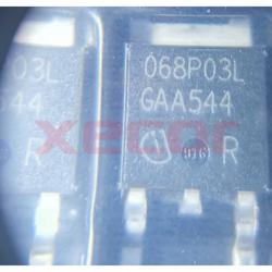
IPD068P03L3GATMA1
MOSFET TRENCH <= 40V
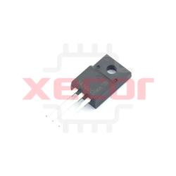
IPA50R500CE
Trans MOSFET N-CH 500V 11.1A 3-Pin(3+Tab) TO-220FP Tube

IPA90R800C3
MOSFET N-Ch 900V 6.9A TO220FP-3 CoolMOS C3
IPB033N10N5LFATMA1
Trans MOSFET N-CH 100V 159A 3-Pin(2+Tab) D2PAK T/R
IPB015N08N5ATMA1
MOSFET N-Ch 80V 180A D2PAK-7 MOSFET MetalOxideSemiconductorFieldEffectTransistor

IPB010N06NATMA1
MOSFET N-Ch 60V 180A D2PAK-6