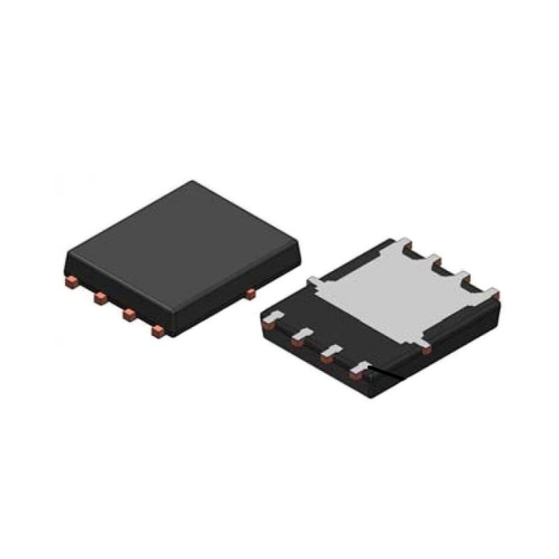
FDMS3668S
Trans MOSFET N-CH 30V 13A/18A 8-Pin Power 56 T/R
| Quantity | Unit Price(USD) | Ext. Price |
|---|---|---|
| 1 | $1.864 | $1.86 |
| 200 | $0.721 | $144.20 |
| 500 | $0.697 | $348.50 |
| 1000 | $0.685 | $685.00 |
Inventory:5,022
- 90-day after-sales guarantee
- 365 Days Quality Guarantee
- Genuine Product Guarantee
- 7*24 hours service quarantee
-
Part Number : FDMS3668S
-
Package/Case : PQFN-8
-
Brands : ON SEMICONDUCTOR
-
Components Categories : MOSFET
-
Datesheet : FDMS3668S DataSheet (PDF)
Overview of FDMS3668S
This device includes two specialized N-Channel MOSFETs in a dual PQFN package. The switch node has been internally connected to enable easy placement and routing of synchronous buck converters. The control MOSFET (Q1) and synchronousSyncFET (Q2) have been designed to provide optimal power efficiency.
Key Features
- Q1: N-Channel
Max rDS(on) = 8 mΩ at VGS = 10 V, ID = 13 A
Max rDS(on) = 11 mΩ at VGS = 4.5 V, ID = 11 A - Q2: N-Channel
Max rDS(on) = 5 mΩ at VGS = 10 V, ID = 18 A
Max rDS(on) = 5.2 mΩ at VGS = 4.5 V, ID = 17 A - Low inductance packaging shortens rise/fall times, resulting in lower switching losses
- MOSFET integration enables optimum layout for lower circuit inductance and reduced switching node ringing
- RoHS Compliant
Application
- Notebook PC
Specifications
The followings are basic parameters of the part selected concerning the characteristics of the part and categories it belongs to.
| Source Content uid | FDMS3668S | Pbfree Code | Yes |
| Part Life Cycle Code | End Of Life | Ihs Manufacturer | ON SEMICONDUCTOR |
| Package Description | QFN-8 | Manufacturer Package Code | 483AJ |
| Reach Compliance Code | not_compliant | ECCN Code | EAR99 |
| Factory Lead Time | 4 Weeks | Samacsys Manufacturer | onsemi |
| Case Connection | DRAIN SOURCE | Configuration | SERIES, 2 ELEMENTS WITH BUILT-IN DIODE |
| DS Breakdown Voltage-Min | 30 V | Drain Current-Max (Abs) (ID) | 60 A |
| Drain Current-Max (ID) | 13 A | Drain-source On Resistance-Max | 0.008 Ω |
| FET Technology | METAL-OXIDE SEMICONDUCTOR | Feedback Cap-Max (Crss) | 70 pF |
| JEDEC-95 Code | MO-240AA | JESD-30 Code | R-PDSO-F6 |
| JESD-609 Code | e3 | Moisture Sensitivity Level | 1 |
| Number of Elements | 2 | Number of Terminals | 6 |
| Operating Mode | ENHANCEMENT MODE | Operating Temperature-Max | 150 °C |
| Package Body Material | PLASTIC/EPOXY | Package Shape | RECTANGULAR |
| Package Style | SMALL OUTLINE | Peak Reflow Temperature (Cel) | 260 |
| Polarity/Channel Type | N-CHANNEL | Power Dissipation-Max (Abs) | 2.5 W |
| Surface Mount | YES | Terminal Finish | Tin (Sn) |
| Terminal Form | FLAT | Terminal Position | DUAL |
| Time@Peak Reflow Temperature-Max (s) | 30 | Transistor Application | SWITCHING |
| Transistor Element Material | SILICON |
Warranty & Returns
Warranty, Returns, and Additional Information
-
QA & Return Policy
Parts Quality Guarantee: 365 days
Returns for refund: within 90 days
Returns for Exchange: within 90 days
-
Shipping and Package
Shipping:For example, FedEx, SF, UPS, or DHL.UPS, or DHL.
Parts Packaging Guarantee: Featuring 100% ESD anti-static protection, our packaging incorporates high toughness and superior buffering capabilities.
-
Payment
For example, channels like VISA, MasterCard, UnionPay, Western Union, PayPal, and more.
If you have specific payment channel preferences or requirements, please get in touch with our sales team for assistance.
Similar Product
FDD4685
channel power field effect transistor, 8.4A, 40V, 0.042ohm, mosfet

FDC6561AN
MOSFET SSOT-6 N-CH 30V

FDC6327C
SuperSOT package with 6 pins
FDC604P
MOSFET SSOT-6 P-CH
FDG6332C
Component type: Trans MOSFET

FDG1024NZ
These MOSFETs offer efficient power handling capabilities with a compact SC-88-6 package design, making them ideal for space-constrained PCB layouts
FDS4141
Trans MOSFET P-CH 40V 10.8A 8-Pin SOIC T/R

FDP12N60NZ
Trans MOSFET N-CH 600V 12A 3-Pin(3+Tab) TO-220 Tube
