Understanding IC 7408: Datasheet, Pin Diagram, and Truth Table
 Prof. David Reynolds
Published:December 31, 2023
In the dynamic realm of electronics, the IC 7408 stands out as a steadfast component, playing a crucial role in digital logic design. The IC 7408, a valuable resource for crafting fundamental logic gates, consists of four AND gates, each equipped with distinct output terminals. Offering the capability to generate a spectrum of basic Boolean functions to intricate logic operations, this adaptable chip facilitates the swift assembly of dependable and user-friendly digital systems. The potential applications of the IC 7408 are virtually boundless, allowing engineers and enthusiasts to translate their concepts promptly into tangible reality. When synergized with additional components, the outcomes can be remarkable, delivering an unmatched blend of convenience and performance.
This article serves as a comprehensive guide for electronics enthusiasts, engineers, and hobbyists, offering insights into the intricacies of the IC 7408. By navigating through the datasheet, interpreting the pin diagram, demystifying the truth table and more details, we explore this quad 2-input AND gate. Join us in uncovering the features, applications, and indispensable contributions of the 7408 IC to the landscape of electronic design. Whether you are a seasoned professional or a curious learner, grasping the subtleties of the 7408 IC promises a journey that illuminates the path to innovation and mastery in electronics.

What is IC 7408?
The IC 7408, belonging to the QUAD 2-Input AND gates, comprises four autonomous gates, each dedicated to performing the logic AND function. Each gate features one output, two inputs, and three pins. Executing the logic AND operation, these gates play a crucial role in digital design. Logic gates are conveniently available as integrated circuits (ICs), with 7408 no exception. Encased in a 14-pin Dual Inline Package (DIP), it is a testament to its robust functionality.
As a cornerstone in digital design, the 7408 Integrated Circuit (IC) is celebrated for its versatility, particularly in constructing fundamental logic gates. Part of the 7400 series of transistor-transistor logic (TTL) chips, it is a quad 2-input AND gate. With four independent gates dedicated to the logical AND function, this IC ensures that its output registers a high signal (logic level 1) only when both input signals are high. Conversely, the output remains low if one or both inputs are low (logic level 0).
Beyond its foundational role in Boolean functions, the 7408 IC's architecture facilitates the execution of intricate logic operations. Its adaptability makes it optimal for quickly developing reliable and user-friendly digital systems. Far surpassing basic applications, this IC's seamless integration with other electronic components can yield remarkable outcomes.
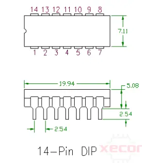
IC 7408 Pin Diagram
The 7408 IC comprises 14 pins, encompassing the ground and Vcc connections. Pin 1 is the initial input for the first AND gate, pin 2 is the second input, and pin 3 represents the output of the first AND gate. Pins 4 to 6 are allocated as inputs and outputs for the second AND gate. Pin 7 acts as the ground connection, supplying power to the chip. At pin 14, the Vcc terminal delivers the necessary power supply to the chip.
The following figure is the IC 7408 pin configuration:

Description of IC 7408 Pin Configuration
| Pin No. | Pin Name | Description |
| 1 | A Input Gate 1 | The first input for the first AND gate |
| 2 | B Input Gate 1 | The second input for the first AND gate |
| 3 | Y Output Gate 1 | The output for the first AND gate |
| 4 | A Input Gate 2 | The first input for the second AND gate |
| 5 | B Input Gate 2 | The second input for the second AND gate |
| 6 | Y Output Gate 2 | The output for the second AND gate |
| 7 | Ground | Connected to the ground or the negative side of the power supply |
| 8 | Y Output Gate 3 | The output for the third AND gate |
| 9 | B Input Gate 3 | The second input for the third AND gate |
| 10 | A Input Gate 3 | The first input for the third AND gate |
| 11 | Y Output Gate 4 | The output for the fourth AND gate |
| 12 | B Input Gate 4 | The second input for the fourth AND gate |
| 13 | A Input Gate 4 | The first input for the fourth AND gate |
| 14 | Vcc - Positive Supply | Connected to the positive side of the power supply |
The 14-pin configuration enables the 7408 IC to accommodate four standalone AND gates, establishing it as a streamlined and effective element for executing logical operations across diverse digital circuits. The dual inline package (DIP) of the IC is meticulously crafted for effortless integration into breadboards or seamless soldering onto printed circuit boards (PCBs). The discernible distinction between input and output pins for each gate on the IC enhances the convenience for circuit designers, allowing the seamless incorporation of the 7408 into intricate designs without signal interference between gates.
Features and Specifications
Features
- Four 2-Input Logic AND Gates: The IC incorporates four autonomous AND gates, each featuring two inputs. This design facilitates the execution of numerous logical operations within a single chip, making it well-suited for intricate digital circuits.
- Compatibility with Various Logic Families: The outputs of the 7408 IC seamlessly interface with diverse logic families, including CMOS (Complementary Metal-Oxide-Semiconductor), NMOS (N-Channel MOSFET), and TTL (Transistor-Transistor Logic). This adaptability is pivotal for integrating into a broad spectrum of digital systems.
- High Noise Immunity: Crafted with a heightened level of noise resistance, the IC 7408 ensures robust functionality in settings characterized by prevalent electrical interference and noise. This attribute bolsters the dependability of the integrated circuit in applications where maintaining signal integrity is paramount, ensuring a steady and reliable operation.
- High-Speed Switching: Renowned for its adeptness in high-speed switching, the IC 7408 facilitates rapid transitions between logic states. This quality proves advantageous in applications requiring prompt response times, such as digital data processing, signal modulation, and real-time control systems.
- Overload Protection: The IC 7408 has protective mechanisms to forestall internal circuitry from excessive currents and voltage fluctuations. This feature augments the robustness of the integrated circuit, rendering it resilient in the face of unforeseen electrical conditions and promoting longevity across diverse applications.
- Low Noise Levels: Boasting low noise levels, the IC 7408 upholds a pristine and stable signal environment. This proves crucial in applications sensitive to extraneous signals or those demanding precise signal processing, such as communication systems, audio amplifiers, and instrumentation circuits. The diminished noise characteristics contribute to elevated signal quality and diminished interference.
- Large Operating Voltage Range: The IC operates effectively across various voltage levels, typically from 4.75V to 5.25V for standard TTL versions. This versatility renders it suitable for diverse power environments, ensuring dependable operation amidst fluctuating power conditions.
- Wide Operating Conditions: Engineered to function in diverse environmental conditions, the IC is well-suited for applications in varied climates and settings. The typical operating temperature ranges from 0°C to 70°C, catering to various operational requirements.
- Legacy Status and Recommendation for New Designs: Although the 7408 has been a mainstay in digital circuit design, it is not endorsed for new designs due to technological advancements and superior alternatives. For contemporary applications, particularly those emphasizing power efficiency and speed, the 74LS08 is recommended. The 74LS08, a low-power Schottky version, offers benefits such as reduced power consumption and faster switching times compared to the standard TTL 7408.
- Fan-out Capability: The IC 7408 can drive multiple inputs in subsequent stages, commonly called fan-out. This feature is pivotal for cascading multiple gates or circuits without additional amplification.
Specifications
- Recommended operating voltage: 5V
- Features 8 input lines and 4 output lines
- Quad 2-input AND gates
- Maximum allowable current draw per gate output: 8mA
- Operating voltage range: 4.75V to 5.25V
- Maximum supply voltage: 7V
- Typical fall time: 18ns
- Typical rise time: 18ns
- Operating temperature range: 0°C to 70°C
- Maximum Propagation Delay Time: 8.7ns
- Input Voltage (High): Minimum 2V (for high-level input)
- Input Voltage (Low): Maximum 0.8V (for low-level input)
- Output Voltage (High): Close to Vcc (when output is high)
- Output Voltage (Low): Close to 0V (when output is low)
- Fan-out: 10 TTL loads
- Propagation Delay: Approximately 10-15 ns
- Power Dissipation: About 10-20 mW per gate
- Package Type: Dual Inline Package (DIP)
Absolute Maximum Ratings
| Supply Voltage | 7V |
| Input Voltage | 5.5V |
| Operating Free Air Temperature | 0°C to +70°C |
| Storage Temperature Range | -65°C to +150°C |
| Maximum Propagation Delay | 10 ns |
| High speed operation | up to 10 MHz |
Observing these utmost ratings is crucial for the appropriate utilization and durability of the IC 7408. Surpassing these thresholds may lead to IC damage or a decline in its performance. Always verify that the operating conditions align with these designated ranges to uphold the IC's reliability and functionality.
- Maximum Signal Propagation Delay: The IC 7408 boasts a 10 nanosecond (ns) peak signal propagation delay. This metric signifies the utmost duration for an alteration in input to manifest at the output, a pivotal factor for timing and synchronization in swift digital circuits.
- Operational Temperature Scope: The IC operates within a temperature span of -55°C to 125°C. This extensive temperature range ensures consistent performance in diverse environmental settings, spanning from severe cold to elevated-temperature scenarios, rendering the IC apt for industrial and military applications.
- Storage Temperature Range: The storage temperature span of -65°C to +150°C permits safe storage of the IC under extreme conditions without impacting its functionality. This broad range proves vital in preserving the long-term integrity of the IC during periods of inactivity.
- High-Velocity Operation: The IC can function at elevated speeds, reaching 10 MHz. This attribute makes it well-suited for high-speed digital applications where swift processing and response times are imperative.
Operating Conditions

Electrical Characteristics

Switching Characteristics

IC 7408 Truth Table
| Input | Output | |
| A | B | Y |
| L | L | L |
| L | H | L |
| H | L | L |
| H | H | H |
The 7408 IC, housing four 2-input AND gates, exhibits a straightforward truth table that mirrors the fundamental logic of an AND gate.
In this table:
- "A" and "B" denote the dual inputs for each AND gate.
- "Y" signifies the output.
- "0" and "1" symbolize the low (0V) and high (typically 5V in TTL logic) logic levels, respectively.
The output (Y) of an AND gate attains a high state (1) solely when both inputs (A and B) are in a high state (1). In all other scenarios—where either or both inputs are in a low state (0)—the output is low (0). This logic prevails across all four AND gates within the 7408 IC.
How Does Circuit 7408 Work?
The integrated circuit 7408, also identified as 74LS08 or simply 08, belongs to the TTL (Transistor-Transistor Logic) family of logic circuits. Widely employed in electronics, this circuit efficiently executes logical AND operations.
Comprising four AND logic gates, each with two inputs labeled A and B and one output denoted Y, the 7408 circuit produces output results based on the logical AND operation between the corresponding inputs.
To comprehend the functioning of the 7408 circuit, understanding the fundamental operation of an AND gate is crucial. An AND gate yields a high output (logic 1) only when both inputs are high. The output becomes low if any of the inputs are low (logical 0).
The 7408 circuit employs bipolar transistors and resistors to realize the AND logic function. Each gate consists of two stages: an input stage and an output stage. The input stage employs a transistor configuration for the AND function, while the output stage employs a transistor to amplify the signal and provide a high output current.
The applications of the 7408 integrated circuit span various areas in electronics, finding frequent use in circuits requiring logical AND operations, such as in control systems, communication systems, and security systems, among others.
Noteworthy advantages of the 7408 circuit include its high switching speed, low power consumption, and wide operating temperature range. Being an integrated circuit, it is user-friendly and easily connectable with other electronic devices.
What Should the Inputs be like in 7408 for the Output to be High?
The 7408 integrated circuit holds significant prominence in electronics for its adeptness in executing logical AND operations. Also recognized as the 7408 chip, this circuit encompasses four AND gates, each featuring two inputs. With two inputs and one output, each gate aims to produce a high output (logic 1) solely when both inputs attain a high state.
In the realm of circuit 7408, for the output of an AND gate to register as high, both inputs necessitate a high state. Here, "high" denotes a logic voltage level corresponding to 1. Should any of the inputs persist in a low state (logic voltage level equivalent to 0), the gate's output assumes a low state (logic 0).
Crucially, compatibility of the inputs in the 7408 circuit with the designated logic voltage levels is paramount. Typically, a 5V voltage source powers the circuit. Consequently, for an AND gate's output to register as high, the inputs demand a voltage exceeding 2.5V, recognized as the threshold for a logic high state.
For optimal performance, incorporating pull-up or pull-down resistors on the inputs of the 7408 circuit is advisable. These resistors guarantee that the inputs assume a defined state without applied external voltage, ensuring the input maintains a high or low logic level.
Moreover, consideration of the propagation time of the 7408 circuit is pivotal. This time span signifies the duration for the output to transition states after input alterations. Influential factors impacting propagation time encompass the capacitive loading of the outputs and the internal gates' capacities. Consequently, when devising circuits incorporating the 7408 IC, accounting for this propagation time proves prudent.
Operation of the 7408 Integrated Circuit

The 7408 integrated circuit operates on TTL technology, utilizing bipolar transistors for logic gate implementation. Each AND gate within the 7408 configuration incorporates two NPN transistors and a pull-up resistor at the output.
Activation of the NPN transistors occurs when both inputs of an AND gate attain a high state, initiating a collector current in each transistor. This current traverses through the pull-up resistor, leading to a high output. Conversely, if any of the inputs register as low, at least one of the NPN transistors deactivates, disrupting the collector current and resulting in low output.
IC 7408 Equivalent
Equivalent alternatives to the IC 7408 include the ICs 74LS08, HEF4081, SN7408, 74HC08, 74HCT08, CD4081, MC14008 and SN54LS08. Either of the two chips can be reconfigured to function as an AND gate. To transform them into an AND gate, the two gate inputs are detached from their original bases. Subsequently, the inputs are linked to buttons, allowing for the alteration of input logic. The output of the AND gate manifests as the voltage across the resistor. This output is then linked to an LED, serving as an indicator to discern the state of the output.
The 74LS08 stands as a widely utilized counterpart to the IC 7408. Renowned for its compatibility with TTL (Transistor-Transistor Logic) circuits, it shares comparable functionality, rendering it a fitting substitute in diverse applications. Its incorporation of four 2-input AND gates aligns seamlessly with the capabilities of the 7408.
HEF4081
The HEF4081 presents another alternative to the IC 7408. This CMOS (Complementary Metal-Oxide-Semiconductor) integrated circuit features four 2-input AND gates, delivering logical operations akin to the 7408. Its low power consumption and versatility make it applicable in various digital logic scenarios.
SN7408
The SN7408, belonging to the 7400 series, is a direct replacement for the IC 7408. Featuring four 2-input AND gates, it exhibits compatibility with TTL logic levels, providing reliability and precision in digital circuits.
Part of the high-speed CMOS series, the 74HC08 offers performance enhancements over its predecessors. While maintaining compatibility with TTL, it delivers improved speed and lower power consumption, positioning itself as a contemporary equivalent for the IC 7408.
The 74HCT08 combines the advantages of high-speed CMOS and TTL technologies, offering enhanced speed and reduced power consumption. It shares the same logical function as the IC 7408, making it a versatile substitute.
The CD4081, a complementary metal-oxide-semiconductor (CMOS) IC, integrates four 2-input AND gates. Its low power consumption and stable performance align with the IC 7408's functionality.
MC14008
The MC14008, a quad 2-input AND gate IC, is a functional equivalent to the IC 7408. Its compatibility with TTL and CMOS logic systems makes it suitable for various digital applications.
SN54LS08
The SN54LS08, a variant of the 74LS08 with similar characteristics, offers low power consumption and compatibility with TTL logic levels, positioning itself as an effective replacement for the IC 7408.
IC 7408 Applications
- Digital Logic Gates
- Binary Counters
- Multiplexers
- Flip-flops
- Bus Driver/Receiver
- Address Decoders
- Data Latches
- Logic Gate Circuits
- Decoders
- Shift Registers
- Counters
- Arithmetic Circuits
- Basic Logic Circuits
- Digital Systems
- Control Systems
- Input/Output Interface
- Signal Gating
- Alarm Systems
- Data Processing
- Educational and Experimental Projects
- Timing Circuits
IC 7408 Price
The pricing of the IC 7408 can fluctuate based on several factors, including the chosen supplier, order quantity, and packaging preferences. Conducting a thorough price comparison across reputable sources is advisable to ensure that you secure the most economically viable deal tailored to your project's specific needs.
When assessing the cost of the IC 7408, it's crucial to consider potential volume discounts available for larger orders. This can significantly impact the overall expenditure and contribute to cost savings, particularly for projects requiring a substantial quantity of these integrated circuits.
Moreover, it is prudent to be attentive to additional charges, such as shipping or handling fees, as these can influence the total procurement cost. Understanding the complete financial picture, including these ancillary expenses, enables a more accurate evaluation of the overall investment required for obtaining the IC 7408 components.
Exploring bundled packages or promotional offers from suppliers is worthwhile in your pursuit of cost-effectiveness. Some vendors may provide discounted rates or package deals that can further optimize your budget allocation without compromising the quality or reliability of the IC 7408 components. This strategic approach to procurement ensures that you obtain the required components and do so in a manner that aligns with your financial considerations and project objectives.
IC 7408 Manufacturer
The 7408 is a widely used integrated circuit (IC) belonging to the 74xx series, a family of digital logic ICs where each member serves a specific logical function. Specifically, the 7408 is classified as a quad 2-input AND gate, each equipped with two inputs, featuring four AND gates.
Various semiconductor companies have been involved in producing ICs within the 74xx series, providing a range of options for users. Here are some notable manufacturers:
Texas Instruments (TI): A prominent semiconductor manufacturer, Texas Instruments is known for producing a diverse array of ICs, including those within the 74xx series.
Fairchild Semiconductor (now part of ON Semiconductor): With a historical presence in IC production, Fairchild Semiconductor, now part of ON Semiconductor, played an early role in manufacturing 74xx series logic ICs.
NXP Semiconductors: Originating from Philips Semiconductors, NXP is recognized for producing logic ICs and contributing to the 74xx series lineup.
STMicroelectronics: As a global semiconductor company, STMicroelectronics manufactures various ICs, encompassing those found in the 74xx series.
When engaging with or procuring the 7408 IC, it's important to note that versions from different manufacturers may be available. However, interchangeability is generally assured as long as these versions adhere to the standard specifications outlined for the 74xx series. This flexibility allows users to choose components from different manufacturers based on availability, pricing, or specific project requirements, providing versatility in sourcing these integral digital logic components.
IC 7408 Datasheet
Download IC 7408 Datasheet.
IC 7408 Package
Dimensional Drawing
Advantages of IC 7408
- Simplicity of Operation
The 7408 integrated circuit, a fundamental digital circuit device, boasts remarkable ease of use. Connecting the input signal to the device's input terminal and linking the output terminal to other digital circuits is the extent of the setup required. Consequently, even individuals new to electronics can navigate its operation effortlessly.
- Cost Efficiency
The widespread use of 7408 integrated circuits contributes to their ready availability at a low cost in the market. This affordability positions it as a highly favored component in digital circuit design.
- Exceptional Reliability
The 7408 integrated circuit embraces a TTL gate design with meticulously selected and matched components. This meticulous approach to design results in exceptional reliability. Consequently, it finds extensive application in highly reliable fields, including industrial control, computer hardware, and electronic instruments.
Conclusion
The 7408 integrated circuit is a fundamental element in digital logic design, recognized for its inclusion of quad 2-input AND gates and reliability within the TTL logic family. Its extensive application across diverse domains, encompassing digital systems, arithmetic operations, and interfacing, positions it as a vital component for individuals involved in electronics, whether enthusiasts, students, or professionals. Proficient comprehension of its pin configuration, operational characteristics, and applications is imperative for unleashing its potential effectively in the design of digital circuits.


FAQ
-
What is the name of the IC 7408?
The IC 7408 is a logic gate chip with four two-input AND gates.
-
Which pin of the IC 7408 is connected to the positive terminal of the power supply to give power?
Pins 7 and 14 provide power to the IC's gate.
-
What is the function of 7408?
The 7408 IC is versatile and can generate simple Boolean functions and intricate logic operations.
-
How many gates are there in 7408?
The 7408 integrated circuit comprises four AND gates, each with two inputs.
-
How many output pins does the 7408 IC component have?
The 7408 is a quad 2-input AND gate housing four distinct gates, each executing the AND logic function. It is presented in a 14-pin DIP package.
-
What is the supply voltage of 7408 IC?
The maximum supply voltage is +7V.

Still, need help? Contact Us: [email protected]