2N5457 N-channel JFET Pinout, Datasheet, Equivalent and Uses
 Dr. James Anderson
Published:January 09, 2024
JFET, a semiconductor device with three terminals, finds applications as amplifiers, voltage-controlled resistors, or electronically-controlled switches. Unlike BJTs, JFETs are entirely voltage-controlled, eliminating the need for biasing current. Various JFET models are available from different manufacturers. One example is the 2N5457 N-channel JFET produced by ON Semiconductor, a company specializing in logic, custom, discrete, signal management, and power devices. They cater to various sectors, including consumer, automotive, industrial, communications, medical, aerospace, military, and LED lighting applications. This article will delve into 2N5457 pinout, circuit diagram, datasheet, equivalent, uses and more details. Everything you need to know about this transistor.

What is 2N5457?
The 2N5457 represents an N-Channel JFET with the unique feature of interchangeable Drain and Source terminals. It is well-suited for a variety of applications involving general-purpose amplification and switching. Functioning in depletion mode necessitates reverse biasing for deactivation since depletion-type MOSFETs mimic a normally closed switch. Notably, it exhibits high input impedance in AC and DC, distinguishing it from other MOSFETs. This device uses CMOS technology to amplify and rapidly switch in low-noise scenarios. The accompanying graph illustrates the common source transfer characteristic, providing valuable insights into the JFET's behavior. This JFET is also applicable for tasks involving switching.

Working Principle of an N-channel JFET transistor
A Junction Field Effect Transistor (JFET) comprises three terminals: Gate, Drain, and Source, with two possible types—N-type and P-type. The illustration below represents an N-type JFET.
In this configuration, the gate terminal is linked to the p substrates, while the source and drain connect to the n substrate, forming a structure akin to two PN junctions. Consequently, depletion regions manifest around the p substrates.
Applying input voltage between the gate and source induces output current collection at the drain terminal. Remarkably, it can be conducted without an input supply. If the gate supply is nil and a positive voltage, surpassing the transistor's pinch-off voltage, is applied between drain and source, it initiates current conduction.
Under forward-biased input junction conditions, the depletion layer diminishes, promoting increased current flow in the drain. Conversely, during reversed biased conditions, the opposite occurs. With this foundational understanding, let's delve into the 2N5457 datasheet analysis.
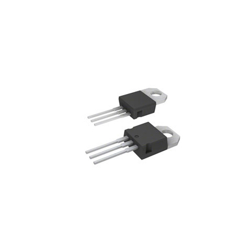
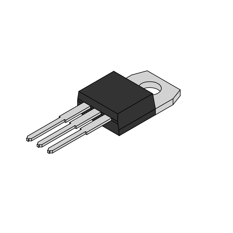
2N5457 Pinout
The pinout configuration of the N-channel JFET, 2N5457, is illustrated in the diagram below.

This silicon transistor with epitaxial construction features three pins. The pin on the left is designated as the drain, while the pin labeled as 3 on the right side functions as the gate. The intermediary pin functions as the source of the JFET.
Pin Configuration
| Pin No. | Pin Name | Description |
| 1 | Drain | Drain pin of the JFET |
| 2 | Source | Source pin of the JFET |
| 3 | Gate | Gate pin of the JFET |
Features & Specifications
Features
- Category: JFET - N - Channel - Depletion
- Application: General Purpose
- N-channel for enhanced gain
- Interchangeable Drain and Source
- Elevated AC input impedance
- Increased DC input resistance
- Minimal transmission and input capacitance
- Reduced cross-modulation and intermodulation distortion
- Encased in a plastic package
- Available with lead-free packaging*
- Optimal for Low Noise & High Gain
- Designed for Transistor Switching Applications
- Operates in Depletion Mode
- Terminal Finish: Tin/Lead
- Mounting Style: Through Hole
Specifications
- Drain-Source Voltage (Vds): 25 Volts
- Drain-Gate Voltage (Vdc): 25 Volts
- Gate-Source Voltage (Vds): -25 Volts
- Power Dissipation: 310 mW
- Gate Current: 10 mA
- Gate-Source Cutoff Voltage (Vds=15 Volts, Id=10 nA): -6.0 Volts
- Cutoff Voltage from Gate to Source ranges from -0.5 to -6.0 Volts.
- Zero Gate Voltage Drain Current (15 Volts, Vgs=0 Volts): 5.0 mA
- Recommended Storage & Operating Temperature: -55 to +150 degrees Celsius
- Package Type: TO-92
- Number of Pins: 3
- Number of Terminations: 3
- Height: 4.7 mm
- Width: 3.68 mm
- Weight: 201 mg
2N5457 Electronic Characteristics

2N5457 Maximum Ratings

2N5457 Equivalent
The equivalents for 2N5457 include 2N5458, J107, J309, and BF246B.
| 2N5458 | It is a direct match for the 2N5457 within the JFET family. Possessing comparable characteristics, the 2N5458 is a dependable alternative suitable for various applications that demand amplification and signal processing. |
| J107 | It's a junction field-effect transistor (JFET), is a compatible substitute for the 2N5457. With specifications and performance closely aligned, it is well-suited for tasks such as pre-amplification, signal switching, and other analog circuit applications. |
| BF246B | It exhibits characteristics resembling those of the 2N5457 in JFET transistors. Its appropriateness for low-power amplification and signal processing aligns with the needs addressed by the 2N5457, rendering it a pragmatic alternative. |
| J309 | Belonging to the JFET family, the J309 can be equivalent to the 2N5457. Offering similar amplification and signal control capabilities, it stands out as a versatile choice applicable to various applications, from audio amplifiers to voltage-controlled oscillators. |
Where & How to Use 2N5457
As previously indicated, the 2N5457 is specifically engineered for amplification applications, making it versatile for enhancing various low-level signals, whether audio or other signal types in electronics. Additionally, it can serve as a switch, capably managing a maximum load of 10mA.
2N5457 - Interfacing Diagram
The image below illustrates the conventional application of the N-Channel JFET 2N5457 as an amplifier.

C1 is the coupling capacitor in the circuit, while C2 is the DC blocking capacitor, capturing the output. The RC, identified as the collector resistor, plays a crucial role in shaping the frequency response and controlling the DC gain by managing the collector current; altering its value affects these parameters. R1 and R2 form a voltage divider to bias the JFET.
For a typical 12V operation, recommended values could be R1 = 100k, R2 = 10k, RC = 10k, with C1 and C2 designated as 1uF ceramic capacitors.
2N5457 Example Circuits
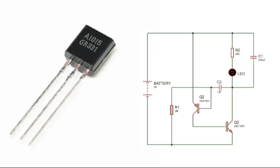
2N5457 Switch Circuit
The schematic illustrates a circuit application utilizing a 2N5457 N-channel JFET as a switch.

An N-channel JFET inherently operates in the "normally on" state, signifying that it activates at zero gate voltage. Furthermore, it doesn't necessitate any biasing voltage for current to flow from drain to source, remaining in saturation mode. The LED illuminates when a voltage source is connected to the LED with no voltage at the JFET's gate terminal. To deactivate the JFET, a negative voltage of sufficient magnitude must be applied to the gate terminal, causing the JFET to transition into the cut-off mode. Consequently, current ceases to flow from drain to source, resulting in the LED losing its luminosity. The incorporated resistor is instrumental in limiting the current through the LED to prevent damage.
2N5457 Chopper circuit
The diagram below illustrates the operational mechanism of JFET functioning as a chopper.

Circuit instability, arising from temperature fluctuations and the coupling of direct and alternating current in amplifiers, can be mitigated by applying choppers.
Subjecting an input DC voltage to a chopper generates an alternating signal with a peak voltage equivalent to the input DC signal. This signal is subsequently amplified using an AC amplifier, preventing undesirable drift. The amplified AC waveform undergoes peak detection to recover the amplified DC output signal.
To induce chopper operation, a square input signal is applied to the gate terminal, causing the JFET to alternate between saturation and cutoff modes.
Similar to the amplification of input DC voltage, the amplification of input AC voltage is achievable without experiencing drift. A low AC input signal is introduced to the chopper, and the resulting waveform is amplified through an AC amplifier, eliminating any drift. The amplified waveform is then subjected to peak detection to restore the original low-input AC signal applied to the chopper.
2N5457 Application
The 2N5457 JFET is primarily employed for amplification, finding application in various scenarios, including:
- Audio preamp circuits
- Amplification of low-level signals
- Sensor circuits
- Amplifier systems
- Audio amplifier stages
- IR detection (Infrared Detection)
- Small switching applications
- Audio modulation
- Tone control
- Noise generator
- Phase-shifting oscillators
- Current limiting systems
How to Safely Long Run in a Circuit
For optimal performance with the 2N5457 JFET, operating within the specified maximum ratings is advisable. Avoid exceeding a load of 10mA, and ensure the load does not surpass 25V across the transistor. The voltage between the drain (D) and gate (G) should not exceed 25V, and the reverse voltage from gate (G) to source (S) should stay below -25V. This transistor's recommended operating and storage temperatures are above -55°C and <+150°C, respectively.
Advantages of 2N5457
The 2N5457 N-channel JFET offers a range of advantages, including:
- Mechanical advantages include being lightweight, being available in compact sizes, featuring a robust shell, and providing effective insulation.
- It is a renowned JFET transistor packaged in TO-92.
- Exhibits high impedance.
- Demonstrates low power consumption.
- Designed in small form factors, minimizing circuit space requirements.
- Characterized by low noise and high gain.
- Functions as a voltage-sensitive device with high input impedance.
- Preferred over BJTs for utilization as the input stage in multi-stage amplifiers.
Feedback Mechanisms and Control Strategies
Effectively utilising the 2N5457 N-channel JFET in your circuits involves thoughtful integration of feedback mechanisms and control strategies. Feedback plays a pivotal role in upholding stability and enhancing overall performance. When working with the 2N5457, it is recommended to incorporate feedback loops to govern signal amplification and maintain reliable operation. Experiment with diverse control strategies, such as voltage-controlled amplifiers, to finely adjust the behaviour of the JFET within distinct circuit setups. A comprehensive grasp and application of these feedback mechanisms will significantly enhance the precision and dependability of your electronic designs.
Potential Issues and Troubleshooting
While the 2N5457 presents versatile applications, users may encounter potential challenges in specific circuit scenarios. Addressing these concerns requires a keen understanding of troubleshooting strategies. Common issues may manifest as signal distortion, biasing problems, or unexpected behavior. If deviations from expected performance arise, systematically analyze the circuit and verify proper biasing and connections. Refer to the datasheet for recommended operating conditions. Additionally, explore alternative resistor values and configurations to troubleshoot and optimize the 2N5457's performance in your particular application. Proactive troubleshooting ensures a seamless integration of the JFET into your electronic projects.
2N5457 Package

2N5457 Datasheet
Download 2N5457 Datasheet PDF.
2N5457 vs 2N5458 vs J201
The table outlines the electrical specifications for 2N5457, 2N5458, and J201, facilitating easy comparison for potential replacements.

While the 2N5457 and 2N5458 JFET devices share nearly identical electrical specifications, slight variations are observed in VGS (OFF), IDSS, power dissipation, and admittance.
The J201, being a distinct JFET device, boasts higher electrical specifications in comparison.
How to Select a JFET
- Begin by selecting the appropriate JFET type for the intended application. For instance, the 2N5457, an N-Channel JFET, is well-suited for use on the low side of the power path. If high-side switching is necessary, opt for a P-Channel JFET.
- Calculate the maximum values for Drain-Source and Gate-Source voltages in the targeted application. Choose a JFET with breakdown voltages for Drain-Source and Gate-Source that exceed the calculated values. The 2N5457, for example, supports a 25V Drain-Source breakdown voltage and a -25V Gate-Source breakdown voltage.
- Determine the maximum Drain Current required for the application. Select a JFET capable of tolerating a Drain current higher than needed. In the case of the 2N5457, it can handle up to 0.005A of continuous Drain current (ID).
Conclusion
The 2N5457 transistor is a versatile element applicable to various electronic circuits. By grasping its pinout and potential applications, you can seamlessly integrate this transistor into your projects, capitalizing on its distinctive features like low noise and high input impedance. Whether an electronics enthusiast or a seasoned professional, the 2N5457 transistor is a valuable asset in your toolkit.
Ensure adherence to the pinout specifications when incorporating the 2N5457 transistor into your circuits, guaranteeing the correct utilization of the gate, drain, and source pins. Armed with this understanding, you can confidently explore the capabilities of the 2N5457 transistor and embark on crafting innovative electronic designs.
Read More

FAQ
-
What is a substitute for 2n5457?
BF245A, 2N5952 (backward), possibly 2N5485, and 2SK30 (dgs pinout) are substitutes for 2n5457.
-
What is the function of the gate pin in the 2N5457 transistor?
In the 2N5457 transistor, the gate pin functions as the control terminal, overseeing the current flow between the source and drain pins by modulating the depletion region's width. Additionally, it provides a high input impedance.
-
What are the advantages of the 2N5457 transistor?
The 2N5457 transistor is well-suited for applications demanding amplification and precise signal control due to its low noise features and elevated input impedance.
-
What does N channel mean?
An N-channel MOSFET is characterized by a MOSFET channel primarily consisting of charge carriers, such as electrons, serving as current carriers.
-
Why is N-channel better than P-channel MOSFET?
The mobility of electrons, acting as carriers in an n-channel device, surpasses that of holes, which serve as carriers in a p-channel device. Consequently, an n-channel device exhibits higher speed compared to a p-channel device.
-
Is N-channel NPN or PNP?
A positive voltage is required at the gate-source for an N-Channel MOSFET to be conducted. Conversely, a P-Channel MOSFET requires a negative Gate-Source voltage for conduction.


Still, need help? Contact Us: [email protected]