
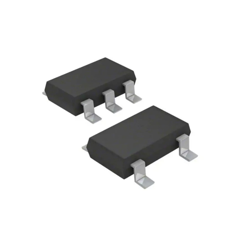
SSM3J15FV,L3F
This MOSFET has a resistance of 12Ω at a current of 10mA and a power dissipation of 150mW at 4V
| Quantity | Unit Price(USD) | Ext. Price |
|---|---|---|
| 1 | $0.060 | $0.06 |
| 200 | $0.024 | $4.80 |
| 500 | $0.023 | $11.50 |
| 1000 | $0.023 | $23.00 |
Inventory:8,457
- 90-day after-sales guarantee
- 365 Days Quality Guarantee
- Genuine Product Guarantee
- 7*24 hours service quarantee
-
Part Number : SSM3J15FV,L3F
-
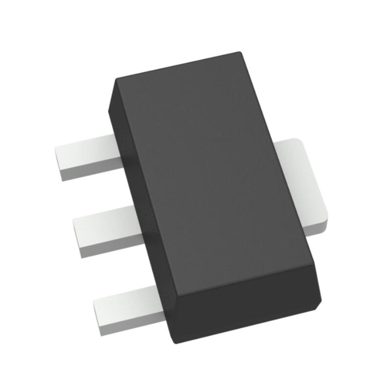
Package/Case : SOT723-3
-
Brand : Toshiba Semiconductor And Storage
-
Components Classification : Single FETs, MOSFETs
-
Datesheet : SSM3J15FV,L3F DataSheet (PDF)
-
Series : Π-MOSVI
The SSM3J15FV,L3F is a P-channel MOSFET transistor with a specified drain-source voltage (VDS) of -20V and continuous drain current (ID) of -0.12A, making it suitable for low-power switching applications. This MOSFET features a compact SOT-23 surface-mount package, providing space-saving benefits for circuit designs. (Note: The pin configuration below is a general representation. Please refer to the datasheet for precise details.) Include a circuit diagram to visualize how the SSM3J15FV,L3F is connected and utilized in a circuit setup. Note: For detailed technical specifications, please consult the SSM3J15FV,L3F datasheet. Functionality The SSM3J15FV,L3F P-channel MOSFET enables efficient power switching with low on-state resistance, making it a versatile component for various low-power applications. Usage Guide Q: What is the maximum drain-source voltage for the SSM3J15FV,L3F? Q: Can the SSM3J15FV,L3F be used in high-power applications? For comparable alternatives to the SSM3J15FV,L3F, consider the following:Overview of SSM3J15FV,L3F
Pinout
Circuit Diagram
Key Features
Application
Frequently Asked Questions
A: The SSM3J15FV,L3F is rated for a maximum drain-source voltage of -20V.
A: No, this MOSFET is designed for low-power switching applications due to its specified current and voltage ratings.Equivalent
Specifications
The followings are basic parameters of the part selected concerning the characteristics of the part and categories it belongs to.
| Product Category | MOSFET | RoHS | Details |
| Technology | Si | Mounting Style | SMD/SMT |
| Package / Case | SOT-723-3 | Transistor Polarity | P-Channel |
| Number of Channels | 1 Channel | Vds - Drain-Source Breakdown Voltage | 30 V |
| Id - Continuous Drain Current | 100 mA | Rds On - Drain-Source Resistance | 12 Ohms |
| Vgs - Gate-Source Voltage | - 20 V, + 20 V | Vgs th - Gate-Source Threshold Voltage | 1.1 V |
| Minimum Operating Temperature | - 55 C | Maximum Operating Temperature | + 150 C |
| Pd - Power Dissipation | 150 mW | Channel Mode | Enhancement |
| Qualification | AEC-Q101 | Tradename | MOSVI |
| Series | SSM3J15 | Brand | Toshiba |
| Configuration | Single | Height | 0.5 mm |
| Length | 1.2 mm | Product Type | MOSFET |
| Factory Pack Quantity | 8000 | Subcategory | MOSFETs |
| Transistor Type | 1 P-Channel | Typical Turn-Off Delay Time | 175 ns |
| Typical Turn-On Delay Time | 65 ns | Width | 0.8 mm |
| Unit Weight | 0.000053 oz |
Warranty & Returns
Warranty, Returns, and Additional Information
-
QA & Return Policy
Parts Quality Guarantee: 365 days
Returns for refund: within 90 days
Returns for Exchange: within 90 days
-
Shipping and Package
Shipping:For example, FedEx, JP, UPS, DHL,SAGAWA, or YTC.
Parts Packaging Guarantee: Featuring 100% ESD anti-static protection, our packaging incorporates high toughness and superior buffering capabilities.
-
Payment
For example, channels like VISA,MasterCard,Western Union,PayPal,MoneyGram,Rakuten Pay and more.
If you have specific payment channel preferences or requirements, please get in touch with our sales team for assistance.

BSS126H6327XTSA2
SOT23 PNP Transistor with 250x Amplification Factor, 45V VCE and 800mA IC Rating

PBSS4350Z,135
NPN3ASOT223PBSS4350Z, PK with 135 of product PBSS4350Z

NSS60600MZ4T1G
Trans GP BJT PNP 60V 6A 2000mW 4-Pin(3+Tab) SOT-223 T/R

MMSS8050-H-TP
This product features a 25V voltage rating and can support a maximum current of 1500mA

BSS123
Trans MOSFET N-CH 100V 0.17A
BSS127H6327XTSA2
N-channel MOSFET with a 21 mA current rating, suitable for a wide variety of electronic applications
BSS138BKS,115
BSS138BKS,115 from Nexperia is a dual N-channel MOSFET designed for applications requiring a maximum current of 320 mA and a voltage of 60 V
BSS131 L6327
Established in 1988 as a leading French electronic distributor
BSS316NH6327XTSA1
N-Channel MOSFET with 30V voltage and 1.4A current in SOT-23-3 package

BSS816NWH6327XTSA1
Tape and reel packaged automotive MOSFET, featuring N-channel technology with a 20V voltage rating and 1
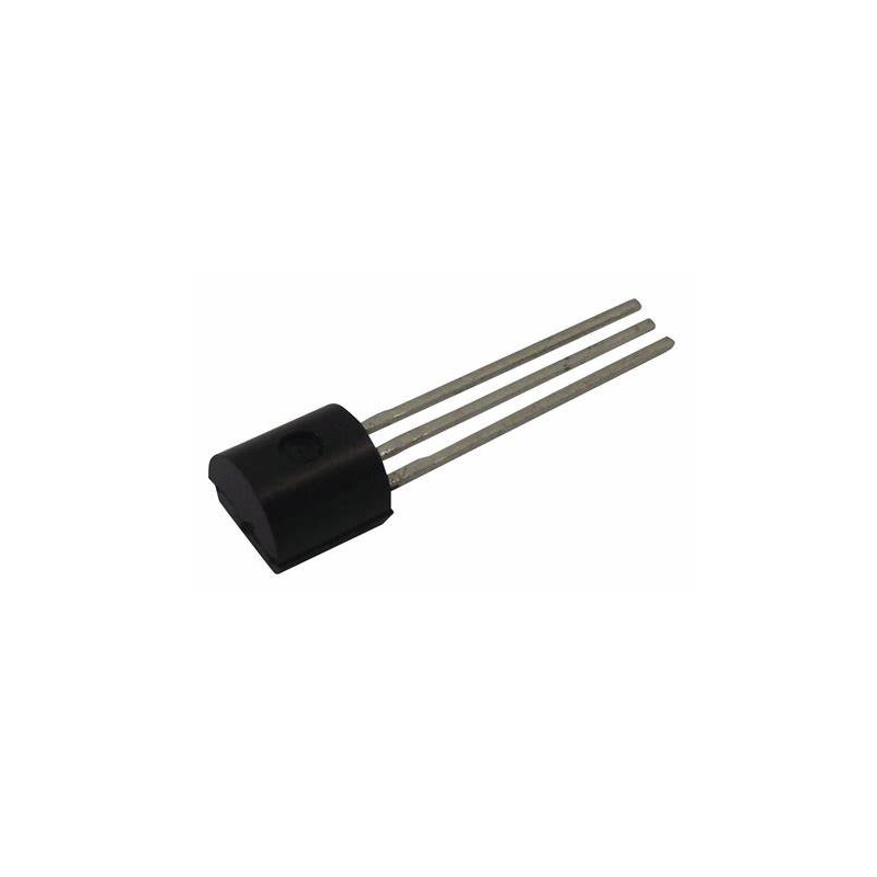
BC546BG
BC546BG is a general purpose BJT with a power dissipation of 625mW and comes in a 3-pin TO-92 package
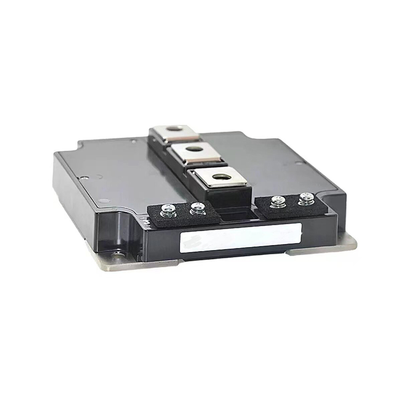
FZ1600R12KF4_S1
FZ1600R12KF4_S1 power module available for US$460.00
TN0604N3-G
N-Channel MOSFET operating in enhancement mode, suitable for 40V with 0.75 Ohm resistance
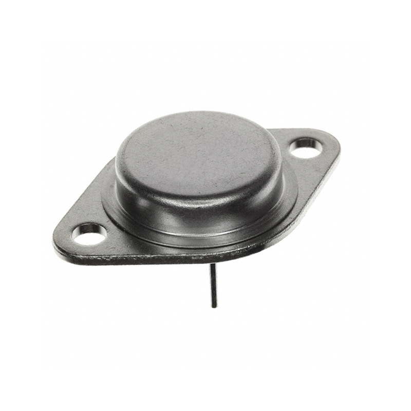
MJ10000
Describing MJ10000

IXTK60N50L2
MOSFET with a 60 Amps and 500V rating
CM300DU-12NFH
Product code: CM300DU-12NFH
IXGH24N60CD1
Power Semiconductor Device with 2.5 Ohms On-Resistance

MS2473
High-power transistor for RF amplificatio
TIM8596-15
High-frequency amplifier for X-band applications, offering reliable performance and hermetic sealin
IXFN48N50U2
SOT-227B-packaged N-channel MOSFET capable of handling 500 volts and 48 amps