
SI3460DDV-T1-GE3
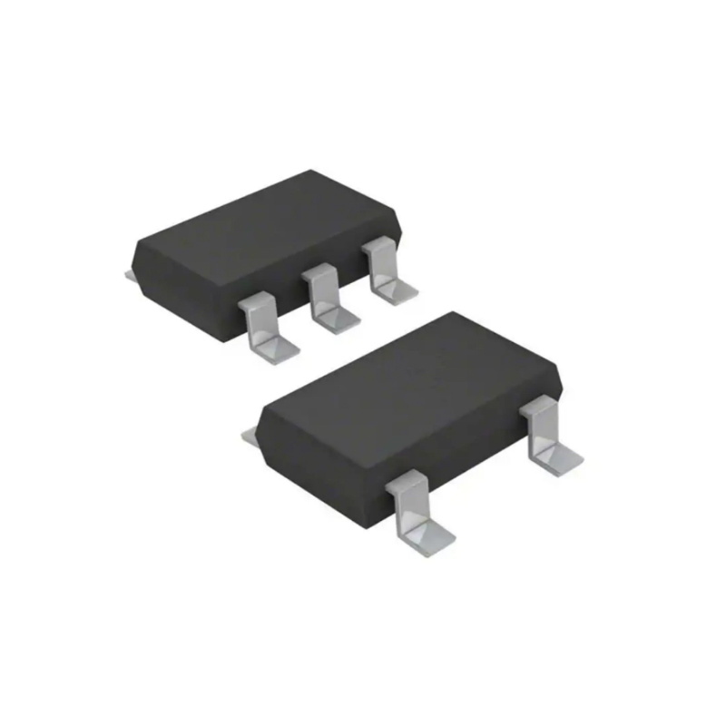
20V N-channel MOSFET capable of handling currents up to 7.9A, housed in a 6-pin TSOP package, supplied in tape and reel format
Inventory:6,210
- 90-day after-sales guarantee
- 365 Days Quality Guarantee
- Genuine Product Guarantee
- 7*24 hours service quarantee
-
Part Number : SI3460DDV-T1-GE3
-
Package/Case : TSOP-6
-
Brands : Siliconix
-
Components Categories : Single FETs, MOSFETs
-
Datesheet : SI3460DDV-T1-GE3 DataSheet (PDF)
-
Series : SI3460DDV
The SI3460DDV-T1-GE3 is a digital controlled variable gain amplifier (DVGA) designed for RF and IF applications. It features a wide gain control range and high linearity, making it suitable for a variety of wireless communication systems. (Note: The pin configuration below is a general representation. Refer to the specific datasheet for precise details.) Include a circuit diagram illustrating the connections and operation of the SI3460DDV-T1-GE3 DVGA for a visual representation. Note: For detailed technical specifications, please refer to the SI3460DDV-T1-GE3 datasheet. Functionality The SI3460DDV-T1-GE3 is a digital controlled variable gain amplifier designed to provide precise gain control and amplification for RF and IF signals. It ensures signal fidelity and optimum performance in wireless communication and signal processing applications. Usage Guide Q: Can the SI3460DDV-T1-GE3 operate from a single supply voltage? For similar functionalities, consider these alternatives to the SI3460DDV-T1-GE3:Overview of SI3460DDV-T1-GE3
Pinout
Circuit Diagram
Key Features
Application
Frequently Asked Questions
A: Yes, the SI3460DDV-T1-GE3 is designed for single supply operation to simplify system integration and power management.Equivalent
Specifications
The followings are basic parameters of the part selected concerning the characteristics of the part and categories it belongs to.
| Product Category | MOSFET | RoHS | Details |
| Technology | Si | Mounting Style | SMD/SMT |
| Package / Case | TSOP-6 | Transistor Polarity | N-Channel |
| Number of Channels | 1 Channel | Vds - Drain-Source Breakdown Voltage | 20 V |
| Id - Continuous Drain Current | 7.9 A | Rds On - Drain-Source Resistance | 28 mOhms |
| Vgs - Gate-Source Voltage | - 8 V, + 8 V | Vgs th - Gate-Source Threshold Voltage | 1 V |
| Qg - Gate Charge | 18 nC | Minimum Operating Temperature | - 55 C |
| Maximum Operating Temperature | + 150 C | Pd - Power Dissipation | 2.7 W |
| Channel Mode | Enhancement | Tradename | TrenchFET |
| Series | SI3 | Brand | Vishay Semiconductors |
| Configuration | Single | Fall Time | 8 ns |
| Height | 1.1 mm | Length | 3.05 mm |
| Product Type | MOSFET | Rise Time | 12 ns |
| Factory Pack Quantity | 3000 | Subcategory | MOSFETs |
| Transistor Type | 1 N-Channel | Typical Turn-Off Delay Time | 21 ns |
| Typical Turn-On Delay Time | 6 ns | Width | 1.65 mm |
| Part # Aliases | SI3460DDV-T1-BE3 SI3460DDV-GE3 | Unit Weight | 0.000705 oz |
Warranty & Returns
Warranty, Returns, and Additional Information
-
QA & Return Policy
Parts Quality Guarantee: 365 days
Returns for refund: within 90 days
Returns for Exchange: within 90 days
-
Shipping and Package
Shipping:For example, FedEx, JP, UPS, DHL,SAGAWA, or YTC.
Parts Packaging Guarantee: Featuring 100% ESD anti-static protection, our packaging incorporates high toughness and superior buffering capabilities.
-
Payment
For example, channels like VISA,MasterCard,Western Union,PayPal,MoneyGram,Rakuten Pay and more.
If you have specific payment channel preferences or requirements, please get in touch with our sales team for assistance.

SI4435DYTRPBF
Power MOSFET with Ultra-Low 0.020 Ohm Resistance Voltage

SIR871DP-T1-GE3
MOSFET -100V Vds 20V Vgs SO-8

SI7232DN-T1-GE3
Dual N-Channel 20 V (D-S) MOSFET SI7232DN-T1-GE3

SI2305CDS-T1-GE3
Small Signal Field-Effect Transistor, P-Channel Silicon MOSFET, 1-Element

SI2337DS-T1-GE3
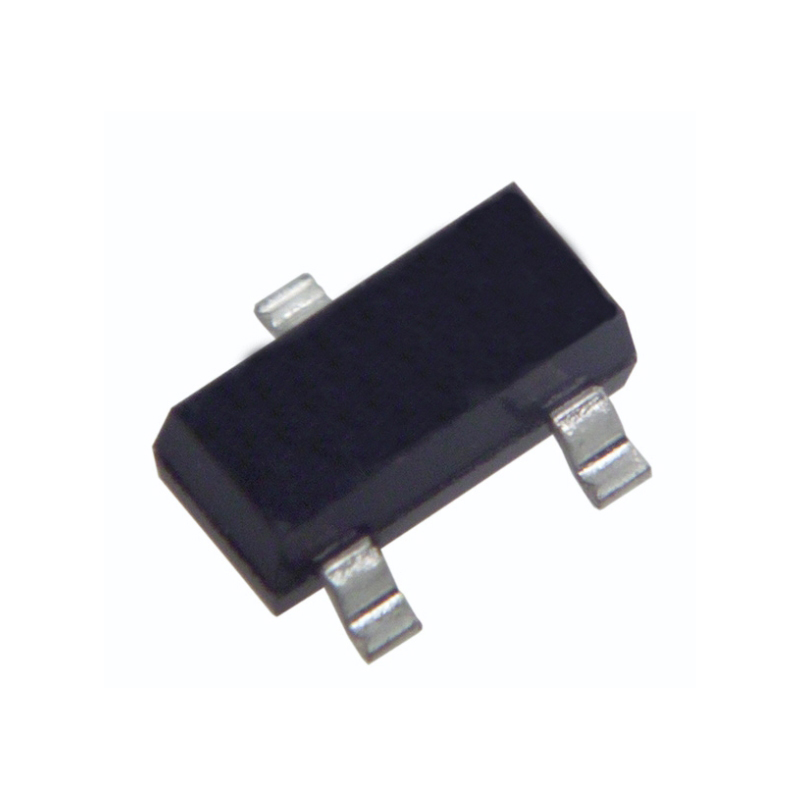
SI2337DS-T1-GE3 P-Channel MOSFET, 1.75 A, 80 V, 3-Pin SOT-23 Vishay

SI7252DP-T1-GE3
SI7252DP-T1-GE3 Power Field-Effect Transistor

SI1304BDL-T1-E3
Recommended Alternative: 78-SI1308EDL-T1-GE3

SI2319DS-T1-E3
Surface-mount device in SOT23 package
SI1013CX-T1-GE3
Packed in a SC-89 package with 3 pins
SI1967DH-T1-GE3
MOSFET with -20V maximum drain-source voltage and 8V gate-source voltage in SC70-6 package