
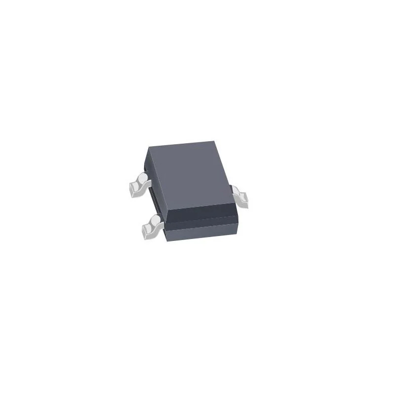
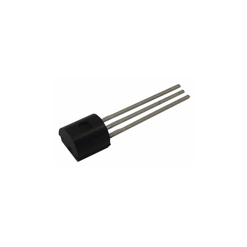
SI1013CX-T1-GE3
Packed in a SC-89 package with 3 pins
Inventory:9,928
- 90-day after-sales guarantee
- 365 Days Quality Guarantee
- Genuine Product Guarantee
- 7*24 hours service quarantee
-
Part Number : SI1013CX-T1-GE3
-
Package/Case : SC-89
-
Brand : Siliconix
-
Components Classification : Single FETs, MOSFETs
-
Datesheet : SI1013CX-T1-GE3 DataSheet (PDF)
-
Series : SI1013CX
The SI1013CX-T1-GE3 is a low-power, low-capacitance MOSFET specifically designed for RF switch applications in mobile devices. This MOSFET features a compact design and high efficiency, making it ideal for RF signal switching in small form factor electronics. (Note: The pin configuration below is a general representation. Refer to the specific datasheet for precise details.) Include a circuit diagram illustrating the connections and operation of the SI1013CX-T1-GE3 MOSFET for a visual representation. Note: For detailed technical specifications, please refer to the SI1013CX-T1-GE3 datasheet. Functionality The SI1013CX-T1-GE3 MOSFET is designed to efficiently switch RF signals in mobile devices, ensuring seamless communication and connectivity. Usage Guide Q: Can the SI1013CX-T1-GE3 be used in high-frequency applications? Q: Is the SI1013CX-T1-GE3 compatible with 5G technology? For similar functionalities, consider these alternatives to the SI1013CX-T1-GE3:Overview of SI1013CX-T1-GE3
Pinout
Circuit Diagram
Key Features
Application
Frequently Asked Questions
A: Yes, the SI1013CX-T1-GE3 is suitable for high-frequency RF signal switching applications with its low capacitance and high efficiency.
A: The SI1013CX-T1-GE3 can be used in 5G devices for RF signal routing and switching, enhancing connectivity and performance.Equivalent
Specifications
The followings are basic parameters of the part selected concerning the characteristics of the part and categories it belongs to.
| Product Category | MOSFET | RoHS | Details |
| Technology | Si | Mounting Style | SMD/SMT |
| Transistor Polarity | P-Channel | Number of Channels | 1 Channel |
| Vds - Drain-Source Breakdown Voltage | 20 V | Id - Continuous Drain Current | 450 mA |
| Rds On - Drain-Source Resistance | 760 mOhms | Vgs - Gate-Source Voltage | - 8 V, + 8 V |
| Vgs th - Gate-Source Threshold Voltage | 1 V | Qg - Gate Charge | 1.65 nC |
| Minimum Operating Temperature | - 55 C | Maximum Operating Temperature | + 150 C |
| Pd - Power Dissipation | 190 mW | Channel Mode | Enhancement |
| Tradename | TrenchFET | Series | SI1 |
| Brand | Vishay Semiconductors | Product Type | MOSFET |
| Factory Pack Quantity | 3000 | Subcategory | MOSFETs |
| Unit Weight | 0.000106 oz |
Warranty & Returns
Warranty, Returns, and Additional Information
-
QA & Return Policy
Parts Quality Guarantee: 365 days
Returns for refund: within 90 days
Returns for Exchange: within 90 days
-
Shipping and Package
Shipping:For example, FedEx, JP, UPS, DHL,SAGAWA, or YTC.
Parts Packaging Guarantee: Featuring 100% ESD anti-static protection, our packaging incorporates high toughness and superior buffering capabilities.
-
Payment
For example, channels like VISA,MasterCard,Western Union,PayPal,MoneyGram,Rakuten Pay and more.
If you have specific payment channel preferences or requirements, please get in touch with our sales team for assistance.

SI4435DYTRPBF
Power MOSFET with Ultra-Low 0.020 Ohm Resistance Voltage

SIR871DP-T1-GE3
MOSFET -100V Vds 20V Vgs SO-8

SI7232DN-T1-GE3
Dual N-Channel 20 V (D-S) MOSFET SI7232DN-T1-GE3

SI2305CDS-T1-GE3
Small Signal Field-Effect Transistor, P-Channel Silicon MOSFET, 1-Element

SI2337DS-T1-GE3
SI2337DS-T1-GE3 P-Channel MOSFET, 1.75 A, 80 V, 3-Pin SOT-23 Vishay

SI7252DP-T1-GE3
SI7252DP-T1-GE3 Power Field-Effect Transistor

SI1304BDL-T1-E3
Recommended Alternative: 78-SI1308EDL-T1-GE3

SI2319DS-T1-E3
Surface-mount device in SOT23 package
LSIC1MO120E0120
Power dissipation rating of 139W at a case temperature of 25°C
IXFX44N60
Through Hole Single N-Channel Power Mosfet - 600 V, 560 W, 330 nC
BS250FTA
MOSFET with P-Type Channel designed to handle up to 45 volts
BSC022N03S
This is the BSC022N03S, a high-performance N-channel MOSFET designed for power applications, capable of handling up to 30 volts and 28 amps."

BSM150GB170DN2
High-Current Dual IGBT Modules with 1700V Voltage Rating
AON7450
AON7450 is an N-channel transistor designed for high voltage and high current applications
IRF9393TRPBF
Product IRF9393TRPBF is a P Channel MOSFET with a voltage rating of 30V, a current rating of 9.2A, and a low on-resistance of 19.4mΩ at 10V
R6046ANZC8
N-Channel Power MOSFET
NTMFS4C029NT1G
Power MOSFET with 30V Voltage Rating and 46A Current Capacity, Single N-Channel, SO-8 FL Package
MPS2222AG
33mm body height
AO6800
Compact and versatile MOSFETs with excellent thermal performance and robust design