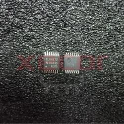
TLV4333IPWR
Op Amp Quad Zero Drift Amplifier R-R I/O ±2.75V/5.5V 14-Pin TSSOP T/R
| Quantity | Unit Price(USD) | Ext. Price |
|---|---|---|
| 1 | $1.442 | $1.44 |
| 10 | $1.242 | $12.42 |
| 30 | $1.117 | $33.51 |
| 100 | $0.982 | $98.20 |
| 500 | $0.924 | $462.00 |
| 1000 | $0.899 | $899.00 |
Inventory:7,062
- 90-day after-sales guarantee
- 365 Days Quality Guarantee
- Genuine Product Guarantee
- 7*24 hours service quarantee
-
Part Number : TLV4333IPWR
-
Package/Case : 14-TSSOP
-
Brands : TI
-
Components Categories : AmplifiersInstrumentation, OP Amps, Buffer Amps
-
Datesheet : TLV4333IPWR DataSheet (PDF)
The TLV4333IPWR is a high-precision, low-power voltage reference IC that provides a stable voltage output for various electronic applications. This IC is designed to offer excellent accuracy and low temperature coefficient, making it suitable for precision measurement and sensor interface systems. (Note: The pin configuration below is a general representation. Refer to the specific datasheet for precise details.) Include a circuit diagram illustrating the connections and operation of the TLV4333IPWR IC for a visual representation. Note: For detailed technical specifications, please refer to the TLV4333IPWR datasheet. Functionality The TLV4333IPWR is a high-precision voltage reference IC that generates a stable output voltage for critical electronic systems, ensuring precise operation and reliable performance. Usage Guide Q: What is the typical output voltage range of the TLV4333IPWR? Q: Is the TLV4333IPWR suitable for precision sensor interfaces? For similar functionalities, consider these alternatives to the TLV4333IPWR:Overview of TLV4333IPWR
Pinout
Circuit Diagram
Key Features
Application
Frequently Asked Questions
A: The TLV4333IPWR typically provides output voltages in the range of 2.5V to 5.0V, depending on the application requirements.
A: Yes, the TLV4333IPWR's high precision and low temperature coefficient make it well-suited for precision sensor interface applications that demand accurate voltage references.Equivalent

Specifications
The followings are basic parameters of the part selected concerning the characteristics of the part and categories it belongs to.
| Source Content uid | TLV4333IPWR | Pbfree Code | Yes |
| Rohs Code | Yes | Part Life Cycle Code | Active |
| Ihs Manufacturer | TEXAS INSTRUMENTS INC | Package Description | TSSOP, |
| Reach Compliance Code | compliant | ECCN Code | EAR99 |
| Samacsys Manufacturer | Texas Instruments | Amplifier Type | OPERATIONAL AMPLIFIER |
| Average Bias Current-Max (IIB) | 0.00013 µA | Bias Current-Max (IIB) @25C | 0.00013 µA |
| Common-mode Reject Ratio-Min | 106 dB | Common-mode Reject Ratio-Nom | 115 dB |
| Input Offset Voltage-Max | 15 µV | JESD-30 Code | R-PDSO-G14 |
| JESD-609 Code | e4 | Length | 5 mm |
| Moisture Sensitivity Level | 2 | Number of Functions | 4 |
| Number of Terminals | 14 | Operating Temperature-Max | 125 °C |
| Operating Temperature-Min | -40 °C | Package Body Material | PLASTIC/EPOXY |
| Package Code | TSSOP | Package Shape | RECTANGULAR |
| Package Style | SMALL OUTLINE, THIN PROFILE, SHRINK PITCH | Peak Reflow Temperature (Cel) | 260 |
| Seated Height-Max | 1.2 mm | Slew Rate-Nom | 0.16 V/us |
| Supply Current-Max | 0.112 mA | Supply Voltage Limit-Max | 7 V |
| Supply Voltage-Nom (Vsup) | 5 V | Surface Mount | YES |
| Technology | CMOS | Temperature Grade | AUTOMOTIVE |
| Terminal Finish | Nickel/Palladium/Gold (Ni/Pd/Au) | Terminal Form | GULL WING |
| Terminal Pitch | 0.65 mm | Terminal Position | DUAL |
| Time@Peak Reflow Temperature-Max (s) | 30 | Unity Gain BW-Nom | 350 |
| Width | 4.4 mm |
Warranty & Returns
Warranty, Returns, and Additional Information
-
QA & Return Policy
Parts Quality Guarantee: 365 days
Returns for refund: within 90 days
Returns for Exchange: within 90 days
-
Shipping and Package
Shipping:For example, FedEx, SF, UPS, or DHL.UPS, or DHL.
Parts Packaging Guarantee: Featuring 100% ESD anti-static protection, our packaging incorporates high toughness and superior buffering capabilities.
-
Payment
For example, channels like VISA, MasterCard, UnionPay, Western Union, PayPal, and more.
If you have specific payment channel preferences or requirements, please get in touch with our sales team for assistance.
Similar Product

TL331IDBVR
Established French Electronics Distributor since 1988

TLC3702IDR
Push-pull output voltage comparator with dual functionality

TLV4172IPWR
10MHzQuad10pATSSOP-1410OperationAmplifierROHS

TLC274CN
This device offers exceptional accuracy and stability, making it ideal for applications that demand reliable signal amplification

TLC272CP
Precision dual LiMCMOS amplifiers

TL082CDR
Product TL082CDR is a dual JFET-input op amp with a 3-MHz bandwidth and a 13-V/μs slew rate

TL084IDR
The TL084IDR offers superior performance and reliability, making it ideal for precision measurement and control systems

TL072ACDR
Low noise amplifier
