
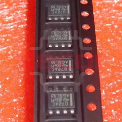
TLV4172IPWR
10MHzQuad10pATSSOP-1410OperationAmplifierROHS
| Quantity | Unit Price(USD) | Ext. Price |
|---|---|---|
| 1 | $1.663 | $1.66 |
| 10 | $1.463 | $14.63 |
| 30 | $1.321 | $39.63 |
| 100 | $1.194 | $119.40 |
| 500 | $1.133 | $566.50 |
| 1000 | $1.110 | $1,110.00 |
Inventory:5,425
- 90-day after-sales guarantee
- 365 Days Quality Guarantee
- Genuine Product Guarantee
- 7*24 hours service quarantee
-
Part Number : TLV4172IPWR
-
Package/Case : TSSOP (PW)-14
-
Brands : TI
-
Components Categories : AmplifiersInstrumentation, OP Amps, Buffer Amps
-
Datesheet : TLV4172IPWR DataSheet (PDF)
Overview of TLV4172IPWR
The TLV4172IPWR is a dual-channel, low-power operational amplifier designed for a wide range of applications including sensor conditioning, battery-powered instrumentation, and data acquisition systems. This device is housed in a small, space-saving package and operates on a supply voltage range of 1.9V to 5.5V, making it suitable for portable and low-power applications.The TLV4172IPWR has a low input bias current of 0.5pA, which helps minimize error in precision applications. It also features a low offset voltage of 400μV, ensuring accurate signal amplification. The amplifier offers a gain bandwidth product of 7 MHz and a slew rate of 3.5V/μs, enabling fast and efficient signal processing.Furthermore, the TLV4172IPWR has a high open-loop gain of 100dB and low noise of 14nV/√Hz, resulting in clear and reliable signal amplification.
Key Features
Application
Specifications
The followings are basic parameters of the part selected concerning the characteristics of the part and categories it belongs to.
| Number of channels | 4 | Total supply voltage (+5 V = 5, ±5 V = 10) (max) (V) | 36 |
| Total supply voltage (+5 V = 5, ±5 V = 10) (min) (V) | 4.5 | Rail-to-rail | In to V-, Out |
| GBW (typ) (MHz) | 10 | Slew rate (typ) (V/µs) | 10 |
| Vos (offset voltage at 25°C) (max) (mV) | 1.7 | Iq per channel (typ) (mA) | 1.6 |
| Vn at 1 kHz (typ) (nV√Hz) | 9 | Rating | Catalog |
| Operating temperature range (°C) | -40 to 125 | Offset drift (typ) (µV/°C) | 1 |
| Features | Cost Optimized, EMI Hardened | CMRR (typ) (dB) | 116 |
| Iout (typ) (A) | 0.075 | Architecture | CMOS |
| Input common mode headroom (to negative supply) (typ) (V) | -0.1 | Input common mode headroom (to positive supply) (typ) (V) | -2 |
| Output swing headroom (to negative supply) (typ) (V) | 0.07 | Output swing headroom (to positive supply) (typ) (V) | -0.07 |
Warranty & Returns
Warranty, Returns, and Additional Information
-
QA & Return Policy
Parts Quality Guarantee: 365 days
Returns for refund: within 90 days
Returns for Exchange: within 90 days
-
Shipping and Package
Shipping:For example, FedEx, SF, UPS, or DHL.UPS, or DHL.
Parts Packaging Guarantee: Featuring 100% ESD anti-static protection, our packaging incorporates high toughness and superior buffering capabilities.
-
Payment
For example, channels like VISA, MasterCard, UnionPay, Western Union, PayPal, and more.
If you have specific payment channel preferences or requirements, please get in touch with our sales team for assistance.
Similar Product

TL331IDBVR
Established French Electronics Distributor since 1988
TLC3702IDR
Push-pull output voltage comparator with dual functionality

TLC274CN
This device offers exceptional accuracy and stability, making it ideal for applications that demand reliable signal amplification

TLC272CP
Precision dual LiMCMOS amplifiers

TL082CDR
Product TL082CDR is a dual JFET-input op amp with a 3-MHz bandwidth and a 13-V/μs slew rate

TL084IDR
The TL084IDR offers superior performance and reliability, making it ideal for precision measurement and control systems
TL072ACDR
Low noise amplifier

TL064CDR
The TL064CDR is a FET input amplifier with a low input offset voltage of 3mV and a high frequency response of 1MHz