
SN74LV4T125RGYR
Buffer gate with 3-state output
Inventory:8,471
- 90-day after-sales guarantee
- 365 Days Quality Guarantee
- Genuine Product Guarantee
- 7*24 hours service quarantee
-
Part Number : SN74LV4T125RGYR
-
Package/Case : VQFN (RGY)-14
-
Brands : TI
-
Components Categories : Buffers, Drivers, Receivers, Transceivers
-
Datesheet : SN74LV4T125RGYR DataSheet (PDF)
The SN74LV4T125RGYR is a quadruple bus buffer gate with 3-state outputs. This IC features a wide operating voltage range and is designed for use in digital signal transmission applications where signal buffering and level shifting are required. (Note: The pin configuration below is a general representation. Refer to the specific datasheet for precise details.) Include a circuit diagram illustrating the connections and operation of the SN74LV4T125RGYR IC for a visual representation. Note: For detailed technical specifications, please refer to the SN74LV4T125RGYR datasheet. Functionality The SN74LV4T125RGYR is designed to buffer and shift signals in digital systems, providing reliable signal transmission and bus sharing capabilities. Usage Guide Q: Can the SN74LV4T125RGYR operate at 5V supply? Q: Is the SN74LV4T125RGYR suitable for bidirectional signal transmission? For similar functionalities, consider these alternatives to the SN74LV4T125RGYR:Overview of SN74LV4T125RGYR
Pinout
Circuit Diagram
Key Features
Application
Frequently Asked Questions
A: Yes, the SN74LV4T125RGYR can operate within a voltage range of 1.65V to 5.5V, making it compatible with 5V systems.
A: Yes, the IC supports bidirectional signal flow with its input/output configurations for each buffer gate.Equivalent
Specifications
The followings are basic parameters of the part selected concerning the characteristics of the part and categories it belongs to.
| Technology family | LV-A | Bits (#) | 4 |
| High input voltage (min) (V) | 1 | High input voltage (max) (V) | 5.5 |
| Vout (min) (V) | 19 | Vout (max) (V) | 5.5 |
| Data rate (max) (MBps) | 100 | IOH (max) (mA) | -16 |
| IOL (max) (mA) | -16 | Supply current (max) (µA) | 5.5 |
| Features | 12.25, 32 | Input type | TTL-Compatible CMOS |
| Output type | 3-State, Balanced CMOS | Operating temperature range (°C) | -40 to 125 |
Warranty & Returns
Warranty, Returns, and Additional Information
-
QA & Return Policy
Parts Quality Guarantee: 365 days
Returns for refund: within 90 days
Returns for Exchange: within 90 days
-
Shipping and Package
Shipping:For example, FedEx, SF, UPS, or DHL.UPS, or DHL.
Parts Packaging Guarantee: Featuring 100% ESD anti-static protection, our packaging incorporates high toughness and superior buffering capabilities.
-
Payment
For example, channels like VISA, MasterCard, UnionPay, Western Union, PayPal, and more.
If you have specific payment channel preferences or requirements, please get in touch with our sales team for assistance.
Similar Product
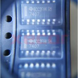
SN7407DR
High-voltage open-collector output configuration
SN74HC14PWR
Inverter Schmitt Trigger 6-Element CMOS 14-Pin TSSOP T/R

SN74LVC1G126DCKR
Buffer/Line Driver 1-CH Non-Inverting 3-ST CMOS 5-Pin SC-70 T/R

SN74LVC1G126DBVR
Buffer/Line Driver 1-CH Non-Inverting 3-ST CMOS 5-Pin SOT-23 T/R

SN74LVC2G34DBVR
Buffer 2-CH Non-Inverting Push-Pull CMOS 6-Pin SOT-23 T/R

SN74AHC1G08DCKR
AND Gate 1-Element 2-IN CMOS 5-Pin SC-70 T/R

SN74LVC1G11DCKR
SN74LVC1G11DCKR Product Code

SN74AVC8T245RHLR
The SN74AVC8T245RHLR is an 8-bit bus transceiver with configurable voltage-level shifting and 3-state outputs in a 24-VQFN package