
SN74LVC2G34DBVR
Buffer 2-CH Non-Inverting Push-Pull CMOS 6-Pin SOT-23 T/R
| Quantity | Unit Price(USD) | Ext. Price |
|---|---|---|
| 5 | $0.162 | $0.81 |
| 50 | $0.135 | $6.75 |
| 150 | $0.122 | $18.30 |
| 500 | $0.107 | $53.50 |
| 3000 | $0.082 | $246.00 |
| 6000 | $0.078 | $468.00 |
Inventory:4,705
- 90-day after-sales guarantee
- 365 Days Quality Guarantee
- Genuine Product Guarantee
- 7*24 hours service quarantee
-
Part Number : SN74LVC2G34DBVR
-
Package/Case : SOT-23 (DBV)-6
-
Brands : TI
-
Components Categories : Buffers, Drivers, Receivers, Transceivers
-
Datesheet : SN74LVC2G34DBVR DataSheet (PDF)
Overview of SN74LVC2G34DBVR
The SN74LVC2G34 device is a dual buffer gate designed for 1.65-V to 5.5-V VCC operation. The SN74LVC2G34 device performs the Boolean function Y = A in positive logic.
NanoFree package technology is a major breakthrough in IC packaging concepts, using the die as the package.
This device is fully specified for partial-power-down applications using Ioff. The Ioff circuitry disables the outputs, preventing damaging current backflow through the device when it is powered down.
Key Features
- Available in the Texas Instruments NanoFree Package
- Supports 5.5-V VCC Operation
- Inputs Accept Voltages to 5.5 V
- Maximum tpd of 4.1 ns at 3.3 V
- Low Power Consumption, 10-µA Maximum ICC
- ±24-mA Output Drive at 3.3 V
- Typical VOLP (Output Ground Bounce) <0.8 V at VCC = 3.3 V, TA = 25°C
- Typical VOHV (Output VOH Undershoot) >2 V at VCC = 3.3 V, TA = 25°C
- Ioff Supports Live Insertion, Partial-Power-Down Mode, and Back-Drive Protection
- Can Be Used as a Down Translator to Translate Inputs From a Maximum of 5.5 V Down to the VCC Level
- Latch-Up Performance Exceeds 100 mA Per JESD 78, Class II
- ESD Protection Exceeds JESD 22
- 2000-V Human Body Model (A114-A)
- 200-V Machine Model (A115-A)
- 1000-V Charged-Device Model (C101)
All trademarks are the property of their respective owners.
Application
- Industrial
- Signal Processing
- Audio
- Imaging
- Video & Vision
- Consumer Electronics
- Computers & Computer Peripherals
- RF Communications
- Wireless
Specifications
The followings are basic parameters of the part selected concerning the characteristics of the part and categories it belongs to.
| Technology family | LVC | Supply voltage (min) (V) | 1.65 |
| Supply voltage (max) (V) | 5.5 | Number of channels | 2 |
| IOL (max) (mA) | 32 | Supply current (max) (µA) | 10 |
| IOH (max) (mA) | -32 | Input type | Standard CMOS |
| Output type | Push-Pull | Features | Balanced outputs, Over-voltage tolerant inputs, Partial power down (Ioff), Very high speed (tpd 5-10ns) |
| Rating | Catalog | Operating temperature range (°C) | -40 to 125, -40 to 85 |
Warranty & Returns
Warranty, Returns, and Additional Information
-
QA & Return Policy
Parts Quality Guarantee: 365 days
Returns for refund: within 90 days
Returns for Exchange: within 90 days
-
Shipping and Package
Shipping:For example, FedEx, SF, UPS, or DHL.UPS, or DHL.
Parts Packaging Guarantee: Featuring 100% ESD anti-static protection, our packaging incorporates high toughness and superior buffering capabilities.
-
Payment
For example, channels like VISA, MasterCard, UnionPay, Western Union, PayPal, and more.
If you have specific payment channel preferences or requirements, please get in touch with our sales team for assistance.
Similar Product

SN74154N
4-to-16 Decoder
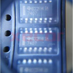
SN7407DR
High-voltage open-collector output configuration
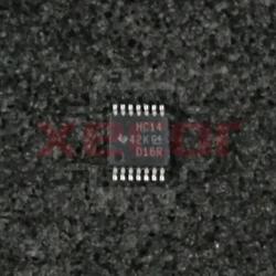
SN74HC14PWR
Inverter Schmitt Trigger 6-Element CMOS 14-Pin TSSOP T/R
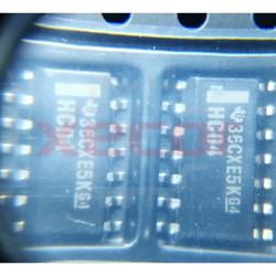
SN74HC04DR
Inverter 6-Element CMOS Automotive 14-Pin SOIC T/R

SN5404J
Contains 6 inverters with a voltage range of 4.5V to 5.5V

SN74AHC14PWR
Inverter Schmitt Trigger 6-Element CMOS 14-Pin TSSOP T/R
SN74LVC1G06DCKR
Buffer/Driver 1-CH Inverting Open Drain CMOS 5-Pin SC-70 T/R
SN74LVC1G32DCKR
Positive logic gates with dual inputs