
LMV358IDR
Op Amp Dual Low Voltage Amplifier R-R O/P 5.5V 8-Pin SOIC T/R
| Quantity | Unit Price(USD) | Ext. Price |
|---|---|---|
| 5 | $0.103 | $0.52 |
| 50 | $0.083 | $4.15 |
| 150 | $0.073 | $10.95 |
| 500 | $0.065 | $32.50 |
| 2500 | $0.057 | $142.50 |
| 4000 | $0.054 | $216.00 |
Inventory:4,048
- 90-day after-sales guarantee
- 365 Days Quality Guarantee
- Genuine Product Guarantee
- 7*24 hours service quarantee
-
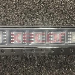
Part Number : LMV358IDR
-
Package/Case : SOIC-8
-
Brands : TI
-
Components Categories : AmplifiersInstrumentation, OP Amps, Buffer Amps
-
Datesheet : LMV358IDR DataSheet (PDF)
The LMV358IDR is a dual operational amplifier IC designed for use in various analog and mixed-signal applications. It features two independent op-amps with high gain bandwidth product and low input offset voltage, making it suitable for precision signal processing. (Note: The pin configuration below is a general representation. Refer to the specific datasheet for precise details.) Include a circuit diagram illustrating the connections and operation of the LMV358IDR IC for a visual representation. Note: For detailed technical specifications, please refer to the LMV358IDR datasheet. Functionality The LMV358IDR is a dual operational amplifier IC that offers high precision and performance for analog signal processing tasks. It is a versatile component for various applications requiring accurate amplification and signal control. Usage Guide Q: What is the typical gain bandwidth product of the LMV358IDR? Q: Can the LMV358IDR operate with a single power supply? For similar functionalities, consider these alternatives to the LMV358IDR:Overview of LMV358IDR
Pinout
Circuit Diagram
Key Features
Application
Frequently Asked Questions
A: The LMV358IDR has a typical gain bandwidth product of 1.2 MHz, allowing for amplification of higher frequency signals.
A: Yes, the LMV358IDR can operate with a single power supply, simplifying circuit design in some applications.Equivalent
Specifications
The followings are basic parameters of the part selected concerning the characteristics of the part and categories it belongs to.
| Number of channels | 2 | Total supply voltage (+5 V = 5, ±5 V = 10) (max) (V) | 5.5 |
| Total supply voltage (+5 V = 5, ±5 V = 10) (min) (V) | 2.7 | Rail-to-rail | In to V-, Out |
| GBW (typ) (MHz) | 1 | Slew rate (typ) (V/µs) | 1 |
| Vos (offset voltage at 25°C) (max) (mV) | 7 | Iq per channel (typ) (mA) | 0.105 |
| Vn at 1 kHz (typ) (nV√Hz) | 39 | Rating | Catalog |
| Operating temperature range (°C) | -40 to 125 | Offset drift (typ) (µV/°C) | 5 |
| Features | Standard Amps | Input bias current (max) (pA) | 250000 |
| CMRR (typ) (dB) | 65 | Iout (typ) (A) | 0.04 |
| Architecture | Bipolar | Input common mode headroom (to negative supply) (typ) (V) | -0.2 |
| Input common mode headroom (to positive supply) (typ) (V) | -0.8 | Output swing headroom (to negative supply) (typ) (V) | 0.065 |
| Output swing headroom (to positive supply) (typ) (V) | -0.12 |
Warranty & Returns
Warranty, Returns, and Additional Information
-
QA & Return Policy
Parts Quality Guarantee: 365 days
Returns for refund: within 90 days
Returns for Exchange: within 90 days
-
Shipping and Package
Shipping:For example, FedEx, SF, UPS, or DHL.UPS, or DHL.
Parts Packaging Guarantee: Featuring 100% ESD anti-static protection, our packaging incorporates high toughness and superior buffering capabilities.
-
Payment
For example, channels like VISA, MasterCard, UnionPay, Western Union, PayPal, and more.
If you have specific payment channel preferences or requirements, please get in touch with our sales team for assistance.
Similar Product
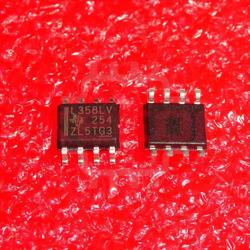
LM358LVIDR
5.5-V voltage range ideal for various circuit designs
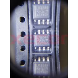
LM358BIDR
Wide temperature range

LM258ADR
This versatile 8-pin SOIC package contains two operational amplifiers that are ideal for a wide range of applications

LM224DR
LM224DR is a ROHS3Compliant op amp with a matte tin finish that operates at 8.65mm
LMV358IDGKR
The LMV358IDGKR is a dual operational amplifier designed for high performance and low power consumption in a wide range of electronic circuits
LMV358IDDUR
Rail-to-rail output
LMC6482AIM/NOPB
SMD Integrated Circuit

LM393N/NOPB
High input impedance