
LMK1C1104PWR
Clock Fanout Buffer 4-OUT 1-IN 1:4 8-Pin TSSOP T/R
Inventory:5,735
- 90-day after-sales guarantee
- 365 Days Quality Guarantee
- Genuine Product Guarantee
- 7*24 hours service quarantee
-
Part Number : LMK1C1104PWR
-
Package/Case : TSSOP-8
-
Brands : TI
-
Components Categories : Clock Buffers, Drivers
-
Datesheet : LMK1C1104PWR DataSheet (PDF)
The LMK1C1104PWR is a precision clock conditioner designed to enhance clock signal quality for various applications. It offers programmable features and high-performance clock distribution, making it ideal for demanding timing solutions. (Note: The pin configuration below is a general representation. Refer to the specific datasheet for precise details.) Include a detailed circuit diagram showcasing the connections and functionality of the LMK1C1104PWR for a visual representation. Note: For detailed technical specifications, please refer to the LMK1C1104PWR datasheet. Functionality The LMK1C1104PWR functions as a clock conditioner, refining input clock signals to provide stable and reliable outputs for various applications that demand precise timing control. Usage Guide Q: Can the LMK1C1104PWR support multiple input clock sources? Q: What is the typical jitter performance of the LMK1C1104PWR? For alternatives with similar capabilities, consider the following products:Overview of LMK1C1104PWR
Pinout
Circuit Diagram
Key Features
Application
Frequently Asked Questions
A: Yes, the LMK1C1104PWR is designed to handle multiple input clock sources and provide conditioned outputs based on the selected configuration.
A: The LMK1C1104PWR offers low jitter performance, ensuring accurate and stable clock signals for precise timing applications.Equivalent
Specifications
The followings are basic parameters of the part selected concerning the characteristics of the part and categories it belongs to.
| Function | Clock buffer, Level translator, Single-ended | Additive RMS jitter (typ) (fs) | 19.2 |
| Output frequency (max) (MHz) | 250 | Number of outputs | 4 |
| Output supply voltage (V) | 1.8, 2.5, 3.3 | Core supply voltage (V) | 1.8, 2.5, 3.3 |
| Output skew (ps) | 25 | Features | 1:4 fanout, Synchronous output enable |
| Operating temperature range (°C) | -40 to 125 | Rating | Catalog |
| Output type | LVCMOS | Input type | LVCMOS |
Warranty & Returns
Warranty, Returns, and Additional Information
-
QA & Return Policy
Parts Quality Guarantee: 365 days
Returns for refund: within 90 days
Returns for Exchange: within 90 days
-
Shipping and Package
Shipping:For example, FedEx, SF, UPS, or DHL.UPS, or DHL.
Parts Packaging Guarantee: Featuring 100% ESD anti-static protection, our packaging incorporates high toughness and superior buffering capabilities.
-
Payment
For example, channels like VISA, MasterCard, UnionPay, Western Union, PayPal, and more.
If you have specific payment channel preferences or requirements, please get in touch with our sales team for assistance.
Similar Product

LMK00334RTVR
4-output clock buffer and level translator for PCIe Gen1/Gen2/Gen3/Gen4/Gen5

LMK1C1102PWR
Clock Buffer 2-channel output LVCMOS 1.8-V buffer 8-TSSOP -40 to 125

LM555H/883
Single Standard Timer TO-99 Tray 8-Pin LM555H/883
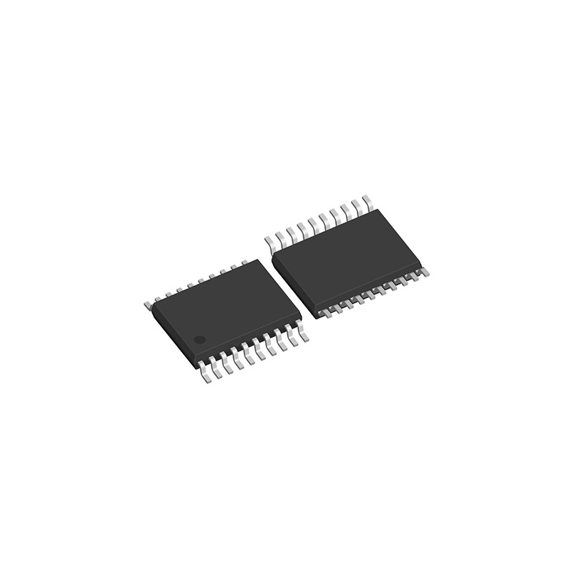
LMK00804BPWR
Clock Fanout Buffer 4-OUT 2-IN 1:4 16-Pin TSSOP T/R
LMK00804BPW
Clock Fanout Buffer 4-OUT 2-IN 1:4 16-Pin TSSOP Tube
LMK00334RTVT
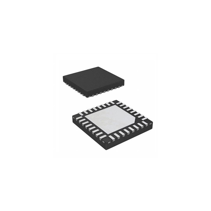
Clock Fanout Buffer 4-OUT 3-IN 1:4 32-Pin WQFN EP T/R
LM555CMMX/NOPB
Standard Timer Single 0°C 70°C 8-Pin VSSOP T/R
LM555CMM/NOPB
Standard Timer Single 0°C 70°C 8-Pin VSSOP T/R