
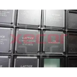
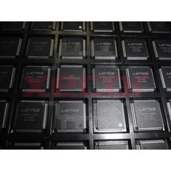
LCMXO2-1200HC-4TG144C
FPGA - Field Programmable Gate Array 1280 LUTs 108 I/O 3.3V -4 SPD
| Quantity | Unit Price(USD) | Ext. Price |
|---|---|---|
| 1 | $7.847 | $7.85 |
| 200 | $3.037 | $607.40 |
| 500 | $2.930 | $1,465.00 |
| 1000 | $2.878 | $2,878.00 |
Inventory:5,665
- 90-day after-sales guarantee
- 365 Days Quality Guarantee
- Genuine Product Guarantee
- 7*24 hours service quarantee
-
Part Number : LCMXO2-1200HC-4TG144C
-
Package/Case : TQFP-144
-
Brands : Lattice Semiconductor Corporation
-
Components Categories : FPGAs (Field Programmable Gate Array)
-
Datesheet : LCMXO2-1200HC-4TG144C DataSheet (PDF)
The LCMXO2-1200HC-4TG144C is a low-cost, low-power FPGA (Field-Programmable Gate Array) featuring 1200 LUTs (Look-Up Tables) and designed for various digital logic applications. It offers a compact and versatile solution for implementing custom logic functions and signal processing algorithms. (Note: The pin configuration below is a general representation. Refer to the specific datasheet for precise details.) Include a circuit diagram illustrating the connections and operation of the LCMXO2-1200HC-4TG144C FPGA for a visual representation. Note: For detailed technical specifications, please refer to the LCMXO2-1200HC-4TG144C datasheet. Functionality The LCMXO2-1200HC-4TG144C FPGA offers a flexible platform for implementing custom logic functions and digital signal processing algorithms. It enables users to design and implement tailored digital solutions according to their specific requirements. Usage Guide Q: Can the LCMXO2-1200HC-4TG144C support real-time signal processing applications? Q: Is the LCMXO2-1200HC-4TG144C suitable for low-power IoT devices? For similar functionalities, consider these alternatives to the LCMXO2-1200HC-4TG144C:Overview of LCMXO2-1200HC-4TG144C
Pinout
Circuit Diagram
Key Features
Application
Frequently Asked Questions
A: Yes, the LCMXO2-1200HC-4TG144C FPGA is capable of handling real-time signal processing tasks effectively, providing flexibility and performance for such applications.
A: Absolutely, the low-power design of the LCMXO2-1200HC-4TG144C makes it an excellent choice for IoT devices requiring customized logic implementations with efficient power utilization.Equivalent
Specifications
The followings are basic parameters of the part selected concerning the characteristics of the part and categories it belongs to.
| Pbfree Code | Yes | Rohs Code | Yes |
| Part Life Cycle Code | Active | Ihs Manufacturer | LATTICE SEMICONDUCTOR CORP |
| Part Package Code | QFP | Package Description | QFP, QFP144,.87SQ,20 |
| Pin Count | 144 | Reach Compliance Code | compliant |
| ECCN Code | EAR99 | HTS Code | 8542.39.00.01 |
| Samacsys Manufacturer | Lattice Semiconductor | Additional Feature | ALSO OPERATES AT 3.3 V NOMINAL SUPPLY |
| Clock Frequency-Max | 133 MHz | JESD-30 Code | S-PQFP-G144 |
| JESD-609 Code | e3 | Length | 20 mm |
| Moisture Sensitivity Level | 3 | Number of Inputs | 107 |
| Number of Logic Cells | 1280 | Number of Outputs | 107 |
| Number of Terminals | 144 | Operating Temperature-Max | 85 °C |
| Operating Temperature-Min | Package Body Material | PLASTIC/EPOXY | |
| Package Code | QFP | Package Equivalence Code | QFP144,.87SQ,20 |
| Package Shape | SQUARE | Package Style | FLATPACK |
| Packing Method | TRAY | Peak Reflow Temperature (Cel) | 260 |
| Power Supplies | 2.5/3.3 V | Programmable Logic Type | FIELD PROGRAMMABLE GATE ARRAY |
| Qualification Status | Not Qualified | Seated Height-Max | 1.6 mm |
| Supply Voltage-Max | 3.465 V | Supply Voltage-Min | 2.375 V |
| Supply Voltage-Nom | 2.5 V | Surface Mount | YES |
| Temperature Grade | OTHER | Terminal Finish | Matte Tin (Sn) |
| Terminal Form | GULL WING | Terminal Pitch | 0.5 mm |
| Terminal Position | QUAD | Time@Peak Reflow Temperature-Max (s) | 30 |
| Width | 20 mm |
Warranty & Returns
Warranty, Returns, and Additional Information
-
QA & Return Policy
Parts Quality Guarantee: 365 days
Returns for refund: within 90 days
Returns for Exchange: within 90 days
-
Shipping and Package
Shipping:For example, FedEx, SF, UPS, or DHL.UPS, or DHL.
Parts Packaging Guarantee: Featuring 100% ESD anti-static protection, our packaging incorporates high toughness and superior buffering capabilities.
-
Payment
For example, channels like VISA, MasterCard, UnionPay, Western Union, PayPal, and more.
If you have specific payment channel preferences or requirements, please get in touch with our sales team for assistance.
Similar Product

LCMXO2-1200HC-4TG144I
FPGA - Field Programmable Gate Array 1280 LUTs 108 I/O 3.3V -4 SPD

LCMXO2-1200HC-4TG100I
FPGA - Field Programmable Gate Array 1280 LUTs 80 I/O 3.3V -4 SPD
LCMXO2-640UHC-4TG144I
CPLD MachXO2 Family 65nm Technology 2.5V/3.3V 144-Pin TQFP Tray
LCMXO640C-3TN144C
CPLD MachXO Family 320 Macro Cells 1.8V/2.5V/3.3V 144-Pin TQFP Tray
LCMXO640C-3FTN256C
CPLD MachXO Family 320 Macro Cells 1.8V/2.5V/3.3V 256-Pin FTBGA Tray

LCMXO2-256HC-4TG100I
CPLD MachXO2 Family 2.5V/3.3V 100-Pin TQFP Tray

LCMXO256C-3MN100C
CPLD MachXO Family 128 Macro Cells 1.8V/2.5V/3.3V 100-Pin CSBGA
LCMXO2-1200HC-4TG100C
FPGA - Field Programmable Gate Array 1280 LUTs 80 I/O 3.3V -4 SPD