
CSD13202Q2
Trans MOSFET N-CH 12V 22A 6-Pin WSON EP T/R
Inventory:5,456
- 90-day after-sales guarantee
- 365 Days Quality Guarantee
- Genuine Product Guarantee
- 7*24 hours service quarantee
-
Part Number : CSD13202Q2
-
Package/Case : WSON-6
-
Brands : TI
-
Components Categories : FETs, MOSFETsSingle FETs, MOSFETs
-
Datesheet : CSD13202Q2 DataSheet (PDF)
The CSD13202Q2 is a dual N-channel NexFET power MOSFET designed for high efficiency power management applications. It features low on-resistance and high thermal performance, making it ideal for use in power supply systems, motor control, and battery management. (Note: The pin configuration below is a general representation. Refer to the specific datasheet for precise details.) Include a circuit diagram illustrating the connections and operation of the CSD13202Q2 IC for a visual representation. Note: For detailed technical specifications, please refer to the CSD13202Q2 datasheet. Functionality The CSD13202Q2 is designed to efficiently switch high currents with minimal losses, making it a reliable solution for power management in various electronic systems. Usage Guide Q: Is the CSD13202Q2 suitable for automotive applications? For similar functionalities, consider these alternatives to the CSD13202Q2:Overview of CSD13202Q2
Pinout
Circuit Diagram
Key Features
Application
Frequently Asked Questions
A: Yes, the CSD13202Q2 is designed for automotive-grade performance, making it suitable for automotive power systems.Equivalent
Specifications
The followings are basic parameters of the part selected concerning the characteristics of the part and categories it belongs to.
| Source Content uid | CSD13202Q2 | Pbfree Code | Yes |
| Rohs Code | Yes | Part Life Cycle Code | Active |
| Ihs Manufacturer | TEXAS INSTRUMENTS INC | Package Description | SMALL OUTLINE, S-PDSO-N6 |
| Reach Compliance Code | compliant | ECCN Code | EAR99 |
| HTS Code | 8541.29.00.95 | Samacsys Manufacturer | Texas Instruments |
| Additional Feature | AVALANCHE RATED | Avalanche Energy Rating (Eas) | 20 mJ |
| Case Connection | DRAIN | Configuration | SINGLE |
| DS Breakdown Voltage-Min | 12 V | Drain Current-Max (Abs) (ID) | 22 A |
| Drain Current-Max (ID) | 14.4 A | Drain-source On Resistance-Max | 0.0116 Ω |
| FET Technology | METAL-OXIDE SEMICONDUCTOR | Feedback Cap-Max (Crss) | 56 pF |
| JESD-30 Code | S-PDSO-N6 | JESD-609 Code | e4 |
| Moisture Sensitivity Level | 1 | Number of Elements | 1 |
| Number of Terminals | 6 | Operating Mode | ENHANCEMENT MODE |
| Operating Temperature-Max | 150 °C | Operating Temperature-Min | -55 °C |
| Package Body Material | PLASTIC/EPOXY | Package Shape | SQUARE |
| Package Style | SMALL OUTLINE | Peak Reflow Temperature (Cel) | 260 |
| Polarity/Channel Type | N-CHANNEL | Power Dissipation-Max (Abs) | 2.7 W |
| Pulsed Drain Current-Max (IDM) | 76 A | Surface Mount | YES |
| Terminal Finish | NICKEL PALLADIUM GOLD | Terminal Form | NO LEAD |
| Terminal Position | DUAL | Time@Peak Reflow Temperature-Max (s) | 30 |
| Transistor Application | SWITCHING | Transistor Element Material | SILICON |
Warranty & Returns
Warranty, Returns, and Additional Information
-
QA & Return Policy
Parts Quality Guarantee: 365 days
Returns for refund: within 90 days
Returns for Exchange: within 90 days
-
Shipping and Package
Shipping:For example, FedEx, SF, UPS, or DHL.UPS, or DHL.
Parts Packaging Guarantee: Featuring 100% ESD anti-static protection, our packaging incorporates high toughness and superior buffering capabilities.
-
Payment
For example, channels like VISA, MasterCard, UnionPay, Western Union, PayPal, and more.
If you have specific payment channel preferences or requirements, please get in touch with our sales team for assistance.
Similar Product

CSD18504Q5A
The CSD18504Q5A MOSFET is designed for efficient power management applications, offering high performance and reliability in a compact form factor

CSD18503Q5A
Texas Instruments CSD18503Q5A N-channel MOSFET Transistor, 145 A, 40 V, 8-Pin SON
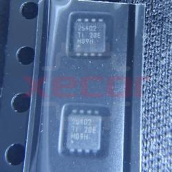
CSD25402Q3A
MOSFET P-CH Pwr MOSFET
CSD19536KTT
CSD19536KTT is a power MOSFET from NexFET™, with N-channel configuration suitable for various applications

CSD19538Q2
Trans MOSFET N-CH Si 100V 14.4A 6-Pin WSON EP T/R

CSD18543Q3A
The specifications of product CSD18543Q3A include a 60-volt N-channel NexFET™ power MOSFET
CSD19532Q5B
MOSFET 100V 4.0 mOhm N-Ch NexFET Power MOSFET
CSD19531Q5A
Trans MOSFET N-CH Si 100V 100A 8-Pin VSONP EP T/R