XS3A1T3157GSH
Analog Switch/Analog Multiplexer Single 2:1 6-Pin XSON T/R
Inventory:3,991
- 90-day after-sales guarantee
- 365 Days Quality Guarantee
- Genuine Product Guarantee
- 7*24 hours service quarantee
-
Part Number : XS3A1T3157GSH
-
Package/Case : XSON-6
-
Brands : Nexperia
-
Components Categories : Analog Switches, Multiplexers, Demultiplexers
-
Datesheet : XS3A1T3157GSH DataSheet (PDF)
Overview of XS3A1T3157GSH
The XS3A1T3157 is a low-ohmic single-pole double-throw analog switch suitable for use as an analog or digital 2:1 multiplexer/demultiplexer. It has a digital select input (S), two independent inputs/outputs (Y1 and Y2) and a common input/output (Z).Schmitt trigger action at the digital input makes the circuit tolerant to slower input rise and fall times. Low threshold digital input allows this device to be driven by 1.8 V logic levels in 3.3 V applications without significant increase in supply current I. This makes it possible for the XS3A1T3157 to switch 4.3 V signals with a 1.8 V digital controller, eliminating the need for logic level translation. The XS3A1T3157 allows signals with amplitude up to V to be transmitted from Z to Y1 or Y2, or from Y1 or Y2 to Z. It's low ON resistance (0.5 Ω) and flatness (0.13 Ω) ensures minimal attenuation and distortion of transmitted signals.
Key Features
- Wide supply voltage range from 1.4 V to 4.3 V
- Very low ON resistance (peak):1.6 Ω (typical) at VCC = 1.4 V1.0 Ω (typical) at VCC = 1.65 V0.55 Ω (typical) at VCC = 2.3 V0.50 Ω (typical) at VCC = 2.7 V0.50 Ω (typical) at VCC = 4.3 V
- 1.6 Ω (typical) at VCC = 1.4 V
- 1.0 Ω (typical) at VCC = 1.65 V
- 0.55 Ω (typical) at VCC = 2.3 V
- 0.50 Ω (typical) at VCC = 2.7 V
- 0.50 Ω (typical) at VCC = 4.3 V
- Break-before-make switching
- High noise immunity
- ESD protection:HBM ANSI/ESDA/JEDEC JS-001 exceeds 8000 VCDM ANSI/ESDA/JEDEC JS-002 exceeds 1000 VIEC61000-4-2 contact discharge exceeds 8000 V for switch ports
- HBM ANSI/ESDA/JEDEC JS-001 exceeds 8000 V
- CDM ANSI/ESDA/JEDEC JS-002 exceeds 1000 V
- IEC61000-4-2 contact discharge exceeds 8000 V for switch ports
- CMOS low-power consumption
- Latch-up performance exceeds 100 mA per JESD78 Class II Level A
- Low-switching threshold levels
- Control input accepts voltages above supply voltage
- Very low supply current, even when input is below VCC
- High current handling capability (350 mA continuous current under 3.3 V supply)
- Specified from -40 °C to +85 °C and from -40 °C to +125 °C
Application
- Mobile phone
- Tablet / Notebook
- Wearables
Specifications
The followings are basic parameters of the part selected concerning the characteristics of the part and categories it belongs to.
| Type number | XS3A1T3157GS | Product status | Production |
| Configuration | SPDT-Z | VCC (V) | 1.4 - 4.3 |
| Logic switching levels | CMOS/LVTTL | RON (Ω) | 0.5 |
| RON(FLAT) (Ω) | 0.2 | f(-3dB) (MHz) | 40 |
| THD (%) | 0.03 | Xtalk (dB) | -90 |
| Power dissipation considerations | ultra low | Tamb (°C) | -40~125 |
| Rth(j-a) (K/W) | 247 | Rth(j-c) (K/W) | 193 |
| Package name | XSON6 | Packing | SOT1202_125 |
| Orderable part number | XS3A1T3157GSH | Chemical content | XS3A1T3157GS |
Warranty & Returns
Warranty, Returns, and Additional Information
-
QA & Return Policy
Parts Quality Guarantee: 365 days
Returns for refund: within 90 days
Returns for Exchange: within 90 days
-
Shipping and Package
Shipping:For example, FedEx, SF, UPS, or DHL.UPS, or DHL.
Parts Packaging Guarantee: Featuring 100% ESD anti-static protection, our packaging incorporates high toughness and superior buffering capabilities.
-
Payment
For example, channels like VISA, MasterCard, UnionPay, Western Union, PayPal, and more.
If you have specific payment channel preferences or requirements, please get in touch with our sales team for assistance.
Similar Product

FT230XS-U
Microprocessor Circuit
TLE9250XSJXUMA1
CAN 5Mbps Power Down 3.3V/5V Automotive 8-Pin DSO T/R
FT231XS-U
5V powered with 20-pin SSOP packaging

FT201XS-R
USB Interface IC USB to I2C IC SSOP-16

FT220XS-U
FT220XS-U product description
80RXS1632AALGI
Switch ICs - Various 400Gbps 10xN RapidIO 24-Port 48-Lane
XS5A1T4157GWH
7.7Ω 1 SPDT TSSOP-6 Analog Switches/Multiplexers, ROHS Certified
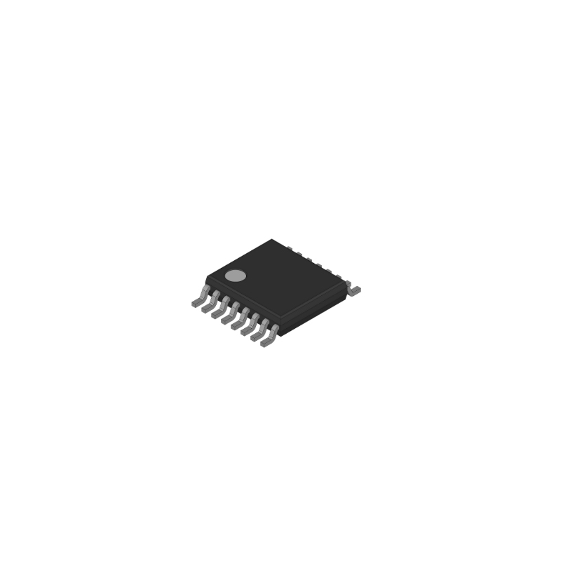
XS3A4052PWJ
ohm dual-throw analog switch

