
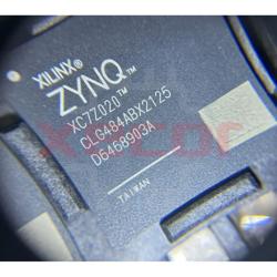
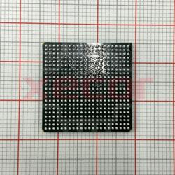
XC7A200T-2FBG676I
Versatile device for a range of applications
| Quantity | Unit Price(USD) | Ext. Price |
|---|---|---|
| 1 | $65.191 | $65.19 |
| 3 | $61.451 | $184.35 |
| 30 | $58.780 | $1,763.40 |
Inventory:8,392
- 90-day after-sales guarantee
- 365 Days Quality Guarantee
- Genuine Product Guarantee
- 7*24 hours service quarantee
-
Part Number : XC7A200T-2FBG676I
-
Package/Case : FCBGA-676
-
Brands : XILINX
-
Components Categories : FPGAs (Field Programmable Gate Array)
-
Datesheet : XC7A200T-2FBG676I DataSheet (PDF)
The XC7A200T-2FBG676I is a high-performance field-programmable gate array (FPGA) featuring a large capacity, advanced architecture, and versatile I/O capabilities. This FPGA is designed to enable rapid prototyping, high-speed processing, and customization for a wide range of applications. (Note: The pin configuration below is a general representation. Refer to the specific datasheet for precise details.) Include a circuit diagram illustrating the connections and operation of the XC7A200T-2FBG676I FPGA for a visual representation. Note: For detailed technical specifications, please refer to the XC7A200T-2FBG676I datasheet. Functionality The XC7A200T-2FBG676I FPGA provides high-speed processing, flexible I/O options, and customization capabilities, making it a versatile solution for a wide range of applications. Usage Guide Q: What is the programming method for the XC7A200T-2FBG676I FPGA? Q: Is the XC7A200T-2FBG676I suitable for real-time signal processing applications? For similar functionalities, consider these alternatives to the XC7A200T-2FBG676I:Overview of XC7A200T-2FBG676I
Pinout
Circuit Diagram
Key Features
Application
Frequently Asked Questions
A: The XC7A200T-2FBG676I FPGA can be programmed using JTAG or SPI interface methods for configuration.
A: Yes, the XC7A200T-2FBG676I FPGA is capable of handling real-time signal processing tasks efficiently.Equivalent
Specifications
The followings are basic parameters of the part selected concerning the characteristics of the part and categories it belongs to.
| Product Category | FPGA - Field Programmable Gate Array | RoHS | Details |
| Series | XC7A200T | Number of Logic Elements | 215360 LE |
| Adaptive Logic Modules - ALMs | 33650 ALM | Embedded Memory | 12.83 Mbit |
| Number of I/Os | 400 I/O | Supply Voltage - Min | 950 mV |
| Supply Voltage - Max | 1.05 V | Minimum Operating Temperature | - 40 C |
| Maximum Operating Temperature | + 100 C | Data Rate | 6.6 Gb/s |
| Number of Transceivers | 8 Transceiver | Mounting Style | SMD/SMT |
| Package / Case | FCBGA-676 | Brand | AMD / Xilinx |
| Distributed RAM | 2888 kbit | Embedded Block RAM - EBR | 13140 kbit |
| Moisture Sensitive | Yes | Number of Logic Array Blocks - LABs | 16825 LAB |
| Operating Supply Voltage | 1 V | Product Type | FPGA - Field Programmable Gate Array |
| Factory Pack Quantity | 1 | Subcategory | Programmable Logic ICs |
| Tradename | Artix | Unit Weight | 5.020543 oz |
Warranty & Returns
Warranty, Returns, and Additional Information
-
QA & Return Policy
Parts Quality Guarantee: 365 days
Returns for refund: within 90 days
Returns for Exchange: within 90 days
-
Shipping and Package
Shipping:For example, FedEx, SF, UPS, or DHL.UPS, or DHL.
Parts Packaging Guarantee: Featuring 100% ESD anti-static protection, our packaging incorporates high toughness and superior buffering capabilities.
-
Payment
For example, channels like VISA, MasterCard, UnionPay, Western Union, PayPal, and more.
If you have specific payment channel preferences or requirements, please get in touch with our sales team for assistance.
Similar Product
XC2C128-7VQG100C
XC2C128-7VQG100C, CPLD CoolRunner II 128 Cells, 80 I/O, 8 Labs, ISP, 1.7 → 1.9 V 100-Pin VTQFP
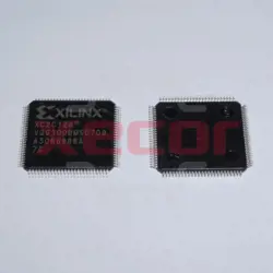
XC7Z020-1CLG484C
Multi-purpose peripheral, Cutting-edge CMOS technology, Quad Flat No-Lead package, Suitable for various applications
XC7S50-1CSGA324I
1098MHz clock frequency
XC6SLX9-3TQG144I
XC6SLX9-3TQG144I is a field-programmable gate array (FPGA) from the Spartan-6 LX family, featuring 9152 cells and built using 45nm CMOS technology
XC6SLX45-3CSG324I
XC6SLX45-3CSG324I is a RoHS compliant product
XC7A200T-2FBG676C
Commercial Grade RoHS compliant for environmentally-friendly operation
XC6SLX45-2FGG484I
High-performance FPGA with 43661 cells

XC3S50AN-4TQG144C
Xilinx XC3S50AN-4TQG144C, FPGA Field Programmable Gate Array Spartan-3AN 1584 Cells, 50000 Gates, 11264bit, 1584 Blocks,