
XC4003E-4PQ100I
FPGA - Field Programmable Gate Array
Inventory:7,871
- 90-day after-sales guarantee
- 365 Days Quality Guarantee
- Genuine Product Guarantee
- 7*24 hours service quarantee
-
Part Number : XC4003E-4PQ100I
-
Package/Case : PQFP-100
-
Brands : Xilinx
-
Components Categories : FPGAs (Field Programmable Gate Array)
-
Datesheet : XC4003E-4PQ100I DataSheet (PDF)
The XC4003E-4PQ100I is a field-programmable gate array (FPGA) from Xilinx, offering programmable logic elements and versatile functionality for digital design. It features 4000 logic cells and 80 I/O pins, making it suitable for a wide range of applications in telecommunications, industrial control, and consumer electronics. (Note: The pin configuration below is a general representation. Refer to the specific datasheet for precise details.) Include a circuit diagram illustrating the connections and operation of the XC4003E-4PQ100I FPGA for a visual representation. Note: For detailed technical specifications, please refer to the XC4003E-4PQ100I datasheet. Functionality The XC4003E-4PQ100I FPGA offers a high level of flexibility and reconfigurability, allowing designers to create customized digital circuits tailored to specific requirements. It enables rapid prototyping and deployment of digital systems with varying complexity. Usage Guide Q: Can the XC4003E-4PQ100I be reprogrammed multiple times? Q: Is the XC4003E-4PQ100I compatible with industry-standard design tools? For similar functionalities, consider these alternatives to the XC4003E-4PQ100I:Overview of XC4003E-4PQ100I
Pinout
Circuit Diagram
Key Features
Application
Frequently Asked Questions
A: Yes, the XC4003E-4PQ100I is a reprogrammable FPGA, allowing users to change the configuration as needed for different applications.
A: Yes, Xilinx provides design software and support for the XC4003E-4PQ100I FPGA, making it compatible with industry-standard design tools for FPGA development.Equivalent
Specifications
The followings are basic parameters of the part selected concerning the characteristics of the part and categories it belongs to.
| Product Category | FPGA - Field Programmable Gate Array | Series | XC4003E |
| Number of Logic Elements | 238 LE | Number of I/Os | 77 I/O |
| Supply Voltage - Min | 3 V | Supply Voltage - Max | 3.6 V |
| Minimum Operating Temperature | - 40 C | Maximum Operating Temperature | + 100 C |
| Mounting Style | SMD/SMT | Package / Case | PQFP-100 |
| Brand | Xilinx | Distributed RAM | 3200 bit |
| Maximum Operating Frequency | 150 MHz | Number of Gates | 3000 |
| Operating Supply Voltage | 3 V to 3.6 V | Product Type | FPGA - Field Programmable Gate Array |
| Subcategory | Programmable Logic ICs |
Warranty & Returns
Warranty, Returns, and Additional Information
-
QA & Return Policy
Parts Quality Guarantee: 365 days
Returns for refund: within 90 days
Returns for Exchange: within 90 days
-
Shipping and Package
Shipping:For example, FedEx, SF, UPS, or DHL.UPS, or DHL.
Parts Packaging Guarantee: Featuring 100% ESD anti-static protection, our packaging incorporates high toughness and superior buffering capabilities.
-
Payment
For example, channels like VISA, MasterCard, UnionPay, Western Union, PayPal, and more.
If you have specific payment channel preferences or requirements, please get in touch with our sales team for assistance.
Similar Product
CY7C64713-128AXC
TQFP-128 packaging

XC6SLX9-3FTG256C
Small and versatile FPGA
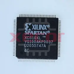
XCS10XL-4VQ100C
96-Cell, CMOS, PBGA144
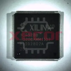
XC95288-15HQ208C
Programmable logic device with 48 macrocells
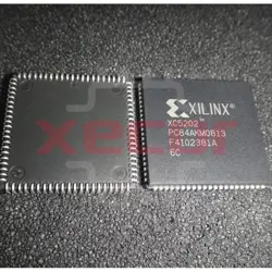
XC5202-6PC84C
This FPGA operates at a frequency of 83MHz and is designed using 0.5um technology

XC3042A-7PC84C
This product is a Programmable Logic IC that utilizes CMOS technology and features SMT for easy installation
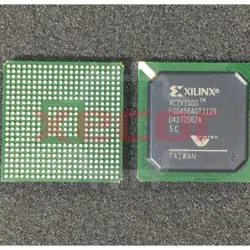
XC2V1000-5FGG456C
XC2V1000-5FGG456C Field Programmable Gate Array
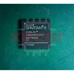
XC6SLX9-2CSG225C
FPGA with 715 CLBs and 667MHz