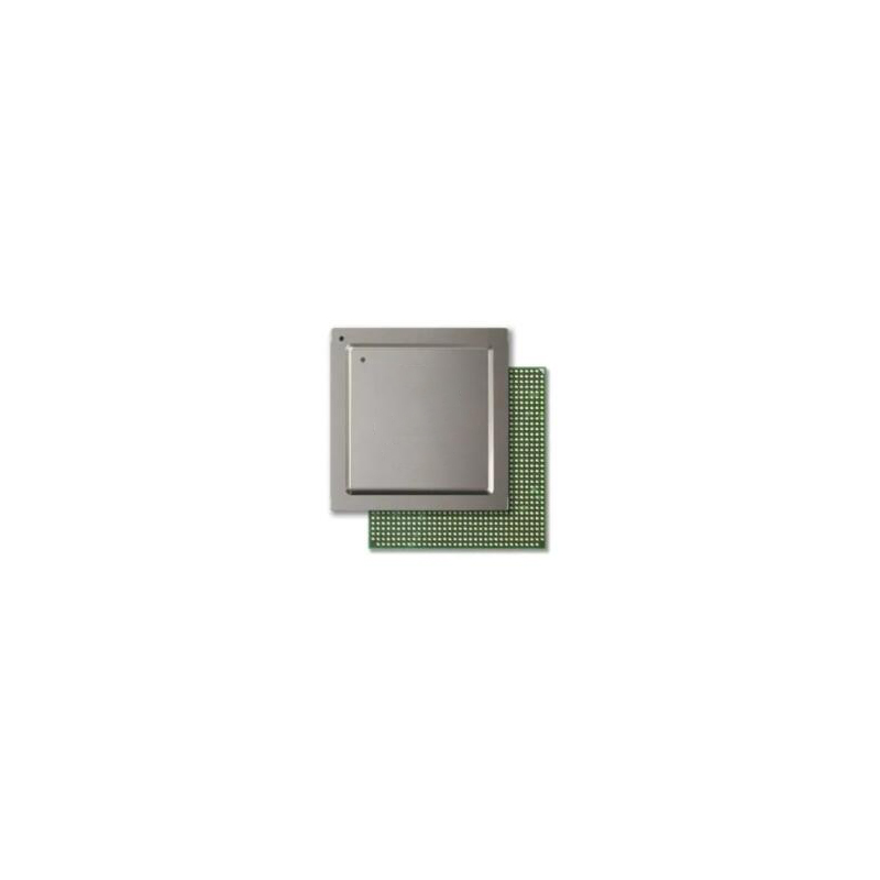
XC2V3000-5FF1152I
FPGA - Field Programmable Gate Array
Inventory:5,577
- 90-day after-sales guarantee
- 365 Days Quality Guarantee
- Genuine Product Guarantee
- 7*24 hours service quarantee
-
Part Number : XC2V3000-5FF1152I
-
Package/Case : 1152-BBGA
-
Brands : AMD
-
Components Categories : FPGAs
-
Datesheet : XC2V3000-5FF1152I DataSheet (PDF)
The XC2V3000-5FF1152I is a Virtex-II FPGA (Field-Programmable Gate Array) from Xilinx, featuring a high logic capacity and versatile programmable capabilities. This FPGA is designed to provide flexible and customizable digital logic implementation for a wide range of applications, from embedded systems to high-performance computing. (Note: The pin configuration below is a general representation. Refer to the specific datasheet for precise details.) Include a circuit diagram illustrating the connections and operation of the XC2V3000-5FF1152I FPGA for a visual representation. Note: For detailed technical specifications, please refer to the XC2V3000-5FF1152I datasheet. Functionality The XC2V3000-5FF1152I FPGA offers customizable logic resources that can be configured to perform a wide range of digital functions. It provides users with a flexible platform for implementing complex digital designs efficiently. Usage Guide Q: Can the XC2V3000-5FF1152I be reprogrammed multiple times? Q: What tools are recommended for programming the XC2V3000-5FF1152I? For similar functionalities, consider these alternatives to the XC2V3000-5FF1152I:Overview of XC2V3000-5FF1152I
Pinout
Circuit DiagramKey Features
Application
Frequently Asked Questions
A: Yes, the Virtex-II FPGA series supports multiple reprogramming cycles, allowing for iterative design changes.
A: Xilinx provides software tools such as Vivado Design Suite for programming and configuring Virtex FPGAs.Equivalent
Specifications
The followings are basic parameters of the part selected concerning the characteristics of the part and categories it belongs to.
| Series | Virtex®-II | Package | Tray |
| Product Status | Obsolete | Programmabe | Not Verified |
| Number of LABs/CLBs | 3584 | Total RAM Bits | 1769472 |
| Number of I/O | 720 | Number of Gates | 3000000 |
| Voltage - Supply | 1.425V ~ 1.575V | Mounting Type | Surface Mount |
| Operating Temperature | -40°C ~ 100°C (TJ) | Package / Case | 1152-BBGA, FCBGA |
| Supplier Device Package | 1152-FCBGA (35x35) | Base Product Number | XC2V3000 |
Warranty & Returns
Warranty, Returns, and Additional Information
-
QA & Return Policy
Parts Quality Guarantee: 365 days
Returns for refund: within 90 days
Returns for Exchange: within 90 days
-
Shipping and Package
Shipping:For example, FedEx, SF, UPS, or DHL.UPS, or DHL.
Parts Packaging Guarantee: Featuring 100% ESD anti-static protection, our packaging incorporates high toughness and superior buffering capabilities.
-
Payment
For example, channels like VISA, MasterCard, UnionPay, Western Union, PayPal, and more.
If you have specific payment channel preferences or requirements, please get in touch with our sales team for assistance.
Similar Product

AT91SAM7XC512-AU
ARM Microcontrollers - MCU LQFP IND TEMP

XC6SLX16-L1CSG225I
FPGA - Field Programmable Gate Array XC6SLX16-L1CSG225I

XC6SLX100T-3FGG484I
FPGA, SPARTAN-6, 296 I/O, FPBGA-484

SAF-XC161CJ-16F40F BB
16-bit Microcontrollers - MCU 16 BIT SNGL CHIP 5V 40MHz Flash

XC5VSX50T-1FFG665I
FPGA - Field Programmable Gate Array XC5VSX50T-1FFG665I

XC5VLX50T-1FFG665I
FPGA - Field Programmable Gate Array Connect to a released FG

XC5VLX85T-1FFG1136C
FPGA - Field Programmable Gate Array BOM fix route to Esperanza Green only Connect to Released FG

XC2S150-5PQG208I
Spartan®-II Field Programmable Gate Array (FPGA) IC 140 49152 3888 208-BFQFP

