
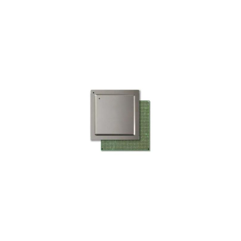
V62/07649-01XA
Enhanced product C6455 fixed point DSP
Inventory:7,504
- 90-day after-sales guarantee
- 365 Days Quality Guarantee
- Genuine Product Guarantee
- 7*24 hours service quarantee
-
Part Number : V62/07649-01XA
-
Package/Case : FCBGA (GTZ)-697
-
Brands : Texas Instruments
-
Components Categories : DSP
-
Datesheet : V62/07649-01XA DataSheet (PDF)
Overview of V62/07649-01XA
The C64x+™ DSPs, such as the SM320C6455-EP device, represent the pinnacle of fixed-point DSP technology within the C6000™ DSP platform. With its advanced VelociTI™ VLIW architecture and 90-nm process technology, the C6455 device delivers unparalleled performance of up to 9600 million instructions per second (MIPS) at a clock rate of 1.2 GHz. This makes it a cost-effective solution for high-performance DSP programming challenges in a variety of applications, including video and telecom infrastructure, imaging/medical, and wireless infrastructure. The device features an impressive eight functional units, integrated Serial RapidIO, and a large on-chip memory system, providing operational flexibility and high-speed data processing capabilities
Key Features
- Controlled Baseline
- One Assembly Site
- Test Site
- One Fabrication Site
- Enhanced Diminishing Manufacturing Sources (DMS) Support
- Enhanced Product-Change Notification
- Qualification Pedigree(1)
- High-Performance Fixed-Point DSP (C6455)
- 1.39 ns, 1.17 ns, 1 ns, and 0.83 ns Instruction Cycle Time
- 1 GHz Clock Rate
- Eight 32 Bit Instructions/Cycle
- 9600 MIPS/MMACS (16 Bits)
- Commercial Temperature (0°C to 90°C)
- Extended Temperature (-40°C to 105°C)
- S-Temp (-55°C to 105°C)
- C64x+™ DSP Core
- Dedicated SPLOOP Instruction
- Compact Instructions (16 Bit)
- Instruction Set Enhancements
- Exception Handling
- C64x+ Megamodule L1/L2 Memory Architecture:
- 256K Bit (32K Byte) L1P Program Cache Direct Mapped)
- 256K Bit (32K Byte) L1D Data Cache 2-Way Set-Associative]
- 16M Bit (2096K Byte) L2 Unified Mapped RAM/Cache (Flexible Allocation)
- 256K Bit (32K Byte) L2 ROM
- Time Stamp Counter
- Enhanced VCP2
- Supports Over 694 7.95 Kbps AMR
- Programmable Code Parameters
- Enhanced Turbo Decoder Coprocessor (TCP2)
- Supports up to Eight 2 Mbps 3GPP (6 Iterations)
- Programmable Turbo Code and Decoding Parameters
- Endianess: Little Endian, Big Endian
- 64 Bit External Memory Interface (EMIFA)
- Glueless Interface to Asynchronous Memories (SRAM, Flash, and EEPROM) and Synchronous Memories (SBSRAM, ZBT SRAM)
- Supports Interface to Standard Sync Devices and Custom Logic (FPGA, CPLD, ASICs, etc.)
- 32M Byte Total Addressable External Memory Space
- Four 1x Serial RapidIO® Links (or One 4x), v1.2 Compliant
- 1.25/2.5/3.125 Gbps Link Rates
- Message Passing, DirectIO Support, Error Management Extensions, and Congestion Control
- IEEE 1149.6 Compliant I/Os
- DDR2 Memory Controller
- Interfaces to DDR2-533 SDRAM
- 32 Bit/16 Bit, 533 MHz (data rate) Bus
- 512M Byte Total Addressable External Memory Space
- EDMA3 Controller (64 Independent Channels)
- 32/16 Bit Host-Port Interface (HPI)
- 32 Bit 33/66 MHz, 3.3 V Peripheral Component Interconnect (PCI) Master/Slave Interface Conforms to PCI Local Bus Specification version 2.3)
- One InterIntegrated Circuit (I2C) Bus
- Two McBSPs
- 10/100/1000 Mb/s Ethernet MAC (EMAC)
- IEEE 802.3 Compliant
- Supports Multiple Media Independent Interfaces (MII, GMII, RMII, and RGMII)
- Eight Independent Transmit (TX) and Eight Independent Receive (RX) Channels
- Two 64 Bit General-Purpose Timers, Configurable as Four 32 Bit Timers
- UTOPIA
- UTOPIA Level 2 Slave ATM Controller
- 8 Bit Transmit and Receive Operations up to 50 MHz per Direction
- User-Defined Cell Format up to 64 Bytes
- 16 General-Purpose I/O (GPIO) Pins
- System PLL and PLL Controller
- Secondary PLL and PLL Controller, Dedicated to EMAC and DDR2 Memory Controller
- Advanced Event Triggering (AET) Compatible
- Trace-Enabled Device
- IEEE-1149.1 (JTAG™) Boundary-Scan-Compatible
- 697-Pin Ball Grid Array (BGA) Package ZTZ or GTZ Suffix), 0.8 mm Ball Pitch
- 0.09 µm/7-Level Cu Metal Process (CMOS)
- 3.3/1.8/1.5/1.25/1.2 V I/Os, 1.25/1.2 V Internal
(1)Component qualification in accordance with JEDEC and industry standards to ensure reliable operation over an extended temperature range. This includes, but is not limited to, Highly Accelerated Stress Test (HAST) or biased 85/85, temperature cycle, autoclave or unbiased HAST, electromigration, bond intermetallic life, and mold compound life. Such qualification testing should not be viewed as justifying use of this component beyond specified performance and environmental limits.
C64x+, JTAG, C64x+, VelociTI, C6000, Code Composer Studio, DSP/BIOS, XDS are trademarks of Texas Instruments.
Specifications
The followings are basic parameters of the part selected concerning the characteristics of the part and categories it belongs to.
| DSP type | 1 C64x | DSP (max) (MHz) | 1000 |
| CPU | 32-/64-bit | Operating system | DSP/BIOS |
| Rating | HiRel Enhanced Product | Operating temperature range (°C) | -55 to 105, 0 to 90 |
Warranty & Returns
Warranty, Returns, and Additional Information
-
QA & Return Policy
Parts Quality Guarantee: 365 days
Returns for refund: within 90 days
Returns for Exchange: within 90 days
-
Shipping and Package
Shipping:For example, FedEx, SF, UPS, or DHL.UPS, or DHL.
Parts Packaging Guarantee: Featuring 100% ESD anti-static protection, our packaging incorporates high toughness and superior buffering capabilities.
-
Payment
For example, channels like VISA, MasterCard, UnionPay, Western Union, PayPal, and more.
If you have specific payment channel preferences or requirements, please get in touch with our sales team for assistance.
Similar Product

P89V664FA
8-bit Microcontrollers - MCU 64K/2K FL ISP/IAP SPI 2XI2C

XCV600E-6HQ240I
FPGA - Field Programmable Gate Array

P89V664FBC,557
8-bit 80C51 5 V low power 16 kB/32 kB/64 kB flash microcontroller with 512 B/1 kB/2 kB RAM, dual I2C-bus, SPI
XC2V6000-5FF1152I
FPGA - Field Programmable Gate Array
XC2V6000-5BF957I
FPGA - Field Programmable Gate Array

XCV600E-6BG432I
FPGA - Field Programmable Gate Array
PIC12HV615-I/SN
Micro 8b, 1.75KB Flash, PIC12HV615-I/SN

V62/14644-01XE
MSP430FR5739 24 MHz ULP microcontroller with 16 KB FRAM, 1 KB SRAM, 32 IO, 10-bit ADC & comparator