
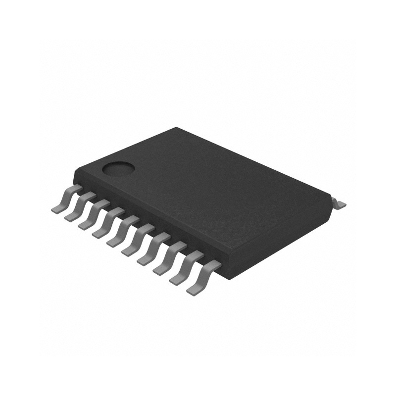
V62/04666-01YE
Buffer/Line Driver 8-CH Non-Inverting 3-ST CMOS 20-Pin TSSOP T/R
Inventory:4,018
- 90-day after-sales guarantee
- 365 Days Quality Guarantee
- Genuine Product Guarantee
- 7*24 hours service quarantee
-
Part Number : V62/04666-01YE
-
Package/Case : TSSOP (PW)-20
-
Brands : Texas Instruments
-
Components Categories : Buffers, Drivers, Receivers, Transceivers
-
Datesheet : V62/04666-01YE DataSheet (PDF)
Overview of V62/04666-01YE
The SN74LVC541A-EP octal buffer/driver is designed for 2.7-V to 3.6-V VCC operation.
The device is ideal for driving bus lines or buffering memory address registers.
This device features inputs and outputs on opposite sides of the package to facilitate printed circuit board layout.
The 3-state control gate is a 2-input AND gate with active-low inputs so that, if either output enable (OE1\ or OE2\) input is high, all eight outputs are in the high-impedance state.
Inputs can be driven from either 3.3-V or 5-V devices. This feature allows the use of this device as a translator in a mixed 3.3-V/5-V system environment.
This device is fully specified for partial-power-down applications using Ioff. The Ioff circuitry disables the outputs, preventing damaging current backflow through the device when it is powered down.
To ensure the high-impedance state during power up or power down, OE\ should be tied to VCC through a pullup resistor; the minimum value of the resistor is determined by the current-sinking capability of the driver.
Key Features
- Controlled Baseline
- One Assembly/Test Site, One Fabrication Site
- Extended Temperature Performance of –40°C to 125°C
- Enhanced Diminishing Manufacturing Sources (DMS) Support
- Enhanced Product-Change Notification
- Qualification Pedigree
- Operates From 2 V to 3.6 V
- Inputs Accept Voltages to 5.5 V
- Max tpd of 5.1 ns at 3.3 V
- Typical VOLP (Output Ground Bounce)
<0.8 V at VCC = 3.3 V, TA = 25°C - Typical VOHV (Output VOH Undershoot)
>2 V at VCC = 3.3 V, TA = 25°C - Supports Mixed-Mode Signal Operation on All Ports (5-V Input/Output Voltage With 3.3-V VCC)
- Ioff Supports Partial-Power-Down Mode Operation
Component qualification in accordance with JEDEC and industry standards to ensure reliable operation over an extended temperature range. This includes, but is not limited to, Highly Accelerated Stress Test (HAST) or biased 85/85, temperature cycle, autoclave or unbiased HAST, electromigration, bond intermetallic life, and mold compound life. Such qualification testing should not be viewed as justifying use of this component beyond specified performance and environmental limits.
Specifications
The followings are basic parameters of the part selected concerning the characteristics of the part and categories it belongs to.
| Technology family | LVC | Supply voltage (min) (V) | 2 |
| Supply voltage (max) (V) | 3.6 | Number of channels | 8 |
| IOL (max) (mA) | 24 | Supply current (max) (µA) | 10 |
| IOH (max) (mA) | -24 | Input type | Standard CMOS |
| Output type | 3-State | Features | Balanced outputs, Very high speed (tpd 5-10ns) |
| Rating | HiRel Enhanced Product | Operating temperature range (°C) | -40 to 125 |
Warranty & Returns
Warranty, Returns, and Additional Information
-
QA & Return Policy
Parts Quality Guarantee: 365 days
Returns for refund: within 90 days
Returns for Exchange: within 90 days
-
Shipping and Package
Shipping:For example, FedEx, SF, UPS, or DHL.UPS, or DHL.
Parts Packaging Guarantee: Featuring 100% ESD anti-static protection, our packaging incorporates high toughness and superior buffering capabilities.
-
Payment
For example, channels like VISA, MasterCard, UnionPay, Western Union, PayPal, and more.
If you have specific payment channel preferences or requirements, please get in touch with our sales team for assistance.
Similar Product
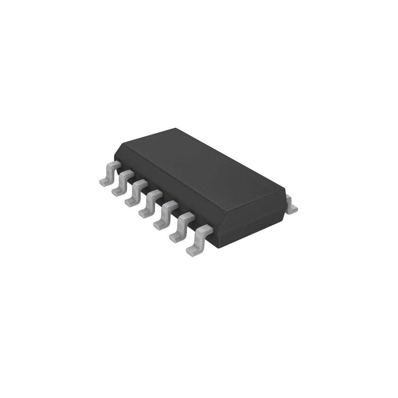
V62/03653-01YE
NAND Gate 4-Element 2-IN CMOS 14-Pin SOIC T/R
V62/03649-01YE
Buffer/Line Driver 8-CH Non-Inverting 3-ST CMOS 20-Pin SOIC T/R
V62/03657-01YE
Buffer/Line Driver 8-CH Non-Inverting 3-ST CMOS 20-Pin SOIC T/R

V62/04602-01YE
Bus XCVR Dual 16-CH 3-ST 48-Pin TSSOP T/R
V62/04679-01XE
Flip Flop D-Type Bus Interface Pos-Edge 3-ST 1-Element 20-Pin TSSOP T/R
V62/04675-01XE
Latch Transparent 3-ST 8-CH D-Type 20-Pin TSSOP T/R
V62/04724-01XE
Buffer/Line Driver 16-CH Non-Inverting 3-ST CMOS 48-Pin TSSOP T/R
V62/04661-02YE
OR Gate 4-Element 2-IN CMOS 14-Pin TSSOP T/R