
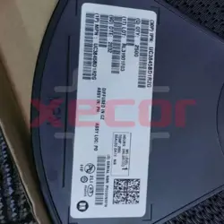
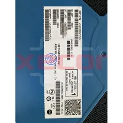
UCC27201DDA
Driver 3A 2-OUT High and Low Side Full Brdg/Half Brdg Non-Inv 8-Pin HSOIC EP Tube
Inventory:2,924
- 90-day after-sales guarantee
- 365 Days Quality Guarantee
- Genuine Product Guarantee
- 7*24 hours service quarantee
-
Part Number : UCC27201DDA
-
Package/Case : HSOIC (DDA)-8
-
Brands : Texas Instruments
-
Components Categories : Gate Drivers
-
Datesheet : UCC27201DDA DataSheet (PDF)
Overview of UCC27201DDA
The UCC2720x family of high-frequency N-channel MOSFET drivers include a 120-V bootstrap diode and high-side and low-side drivers with independent inputs for maximum control flexibility. This allows for N-channel MOSFET control in half-bridge, full-bridge, two-switch forward, and active clamp forward converters. The low-side and the high-side gate drivers are independently controlled and matched to 1 ns between the turnon and turnoff of each other.
An on-chip bootstrap diode eliminates the external discrete diodes. Undervoltage lockout is provided for both the high-side and the low-side drivers forcing the outputs low if the drive voltage is below the specified threshold.
Two versions of the UCC27200 are offered. The UCC27200 has high noise immune CMOS input thresholds while the UCC27201 has TTL compatible thresholds.
Key Features
- Drives Two N-Channel MOSFETs in High-Side
and Low-Side Configuration - Negative Voltage Handling on HS (–5 V)
- Maximum Boot Voltage of 120 V
- Maximum VDD Voltage of 20 V
- On-Chip 0.65-V VF, 0.6-Ω RD Bootstrap Diode
- Greater than 1 MHz of Operation
- 20-ns Propagation Delay Times
- 3-A Sink and 3-A Source Output Currents
- 8-ns Rise and 7-ns Fall Time With 1000-pF Load
- 1-ns Delay Matching
- Undervoltage Lockout for High-Side and Low-Side
Driver - Specified from –40°C to 140°C
Specifications
The followings are basic parameters of the part selected concerning the characteristics of the part and categories it belongs to.
| Bus voltage (max) (V) | 110 | Power switch | MOSFET |
| Input VCC (min) (V) | 8 | Input VCC (max) (V) | 17 |
| Peak output current (A) | 3 | Operating temperature range (°C) | -40 to 140 |
| Undervoltage lockout (typ) (V) | 8 | Rating | Catalog |
| Propagation delay time (µs) | 0.02 | Rise time (ns) | 8 |
| Fall time (ns) | 7 | Iq (mA) | 0.001 |
| Input threshold | TTL | Channel input logic | TTL |
| Negative voltage handling at HS pin (V) | -5 | Driver configuration | Noninverting |
Warranty & Returns
Warranty, Returns, and Additional Information
-
QA & Return Policy
Parts Quality Guarantee: 365 days
Returns for refund: within 90 days
Returns for Exchange: within 90 days
-
Shipping and Package
Shipping:For example, FedEx, SF, UPS, or DHL.UPS, or DHL.
Parts Packaging Guarantee: Featuring 100% ESD anti-static protection, our packaging incorporates high toughness and superior buffering capabilities.
-
Payment
For example, channels like VISA, MasterCard, UnionPay, Western Union, PayPal, and more.
If you have specific payment channel preferences or requirements, please get in touch with our sales team for assistance.
Similar Product

UC3843BVD1R2G
Current Mode Control
UC3845BD1R2G
8-Pin SOIC N T/R
UC2842BD1R2G
Current Mode PWM Controller 1A 500kHz 8-Pin SOIC N T/R

UC3845BD1013TR
Switching Controllers 0.5mA Current Mode
UC3844BD1R2G
Current Mode PWM Controller 1A 500kHz 8-Pin SOIC N T/R

UC3903N
Multi-channel Power Supply Checker
UC3717AN
4.75V~5.25V Half Bridge Gate Drive ICs ROHS in PDIP-16

UC3717AQ
Stepper motor drive circuit for motor, motion, and ignition control