
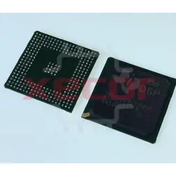
TMS320C6202GLS250
Digital Signal Processors & Controllers - DSP, DSC Fixed-Pt Dig Signal Proc
| Quantity | Unit Price(USD) | Ext. Price |
|---|---|---|
| 1 | $263.893 | $263.89 |
| 200 | $102.123 | $20,424.60 |
| 500 | $98.535 | $49,267.50 |
| 1000 | $96.763 | $96,763.00 |
Inventory:7,102
- 90-day after-sales guarantee
- 365 Days Quality Guarantee
- Genuine Product Guarantee
- 7*24 hours service quarantee
-
Part Number : TMS320C6202GLS250
-
Package/Case : FCBGA-384
-
Brands : TI
-
Components Categories : DSP (Digital Signal Processors)
-
Datesheet : TMS320C6202GLS250 DataSheet (PDF)
The TMS320C6202GLS250 is a digital signal processor (DSP) IC that is part of the Texas Instruments TMS320C62x DSP generation. It features a clock speed of 250MHz and is designed for high-performance signal processing applications. This DSP offers advanced computational capabilities and is ideal for applications requiring real-time processing and high-speed data manipulation. (Note: The pin configuration below is a general representation. Refer to the specific datasheet for precise details.) Include a circuit diagram illustrating the connections and operation of the TMS320C6202GLS250 DSP for a visual representation. Note: For detailed technical specifications, please refer to the TMS320C6202GLS250 datasheet. Functionality The TMS320C6202GLS250 is a high-performance DSP designed for demanding signal processing tasks. It offers efficient computation and processing capabilities for various applications. Usage Guide Q: Can the TMS320C6202GLS250 be overclocked for higher performance? Q: Is the TMS320C6202GLS250 suitable for real-time image processing applications? For similar functionalities, consider these alternatives to the TMS320C6202GLS250:Overview of TMS320C6202GLS250
Pinout
Circuit Diagram
Key Features
Application
Frequently Asked Questions
A: The TMS320C6202GLS250 is designed to operate at 250MHz. Overclocking may lead to instability and is not recommended.
A: Yes, the TMS320C6202GLS250 is well-suited for real-time image processing tasks due to its high-speed processing capabilities.Equivalent
Specifications
The followings are basic parameters of the part selected concerning the characteristics of the part and categories it belongs to.
| Source Content uid | TMS320C6202GLS250 | Pbfree Code | Yes |
| Rohs Code | No | Part Life Cycle Code | Not Recommended |
| Ihs Manufacturer | TEXAS INSTRUMENTS INC | Part Package Code | BGA |
| Package Description | HFBGA, BGA384,22X22,32 | Pin Count | 384 |
| Reach Compliance Code | not_compliant | ECCN Code | 3A991.A.2 |
| HTS Code | 8542.31.00.01 | Date Of Intro | 1998-08-01 |
| Samacsys Manufacturer | Texas Instruments | Additional Feature | ALSO REQUIRES 3.3V SUPPLY |
| Address Bus Width | 22 | Barrel Shifter | NO |
| Bit Size | 32 | Boundary Scan | YES |
| Clock Frequency-Max | 250 MHz | External Data Bus Width | 32 |
| Format | FIXED POINT | Integrated Cache | YES |
| Internal Bus Architecture | MULTIPLE | JESD-30 Code | S-PBGA-B384 |
| JESD-609 Code | e0 | Length | 18 mm |
| Low Power Mode | YES | Moisture Sensitivity Level | 4 |
| Number of DMA Channels | 4 | Number of External Interrupts | 4 |
| Number of Terminals | 384 | Number of Timers | 2 |
| On Chip Data RAM Width | 8 | On Chip Program ROM Width | 8 |
| Operating Temperature-Max | 90 °C | Operating Temperature-Min | |
| Package Body Material | PLASTIC/EPOXY | Package Code | HFBGA |
| Package Equivalence Code | BGA384,22X22,32 | Package Shape | SQUARE |
| Package Style | GRID ARRAY, HEAT SINK/SLUG, FINE PITCH | Peak Reflow Temperature (Cel) | 220 |
| Power Supplies | 1.8,3.3 V | Qualification Status | Not Qualified |
| RAM (words) | 32768 | ROM Programmability | MROM |
| Seated Height-Max | 2.8 mm | Supply Voltage-Max | 1.89 V |
| Supply Voltage-Min | 1.71 V | Supply Voltage-Nom | 1.8 V |
| Surface Mount | YES | Technology | CMOS |
| Temperature Grade | OTHER | Terminal Finish | TIN LEAD |
| Terminal Form | BALL | Terminal Pitch | 0.8 mm |
| Terminal Position | BOTTOM | Time@Peak Reflow Temperature-Max (s) | 20 |
| Width | 18 mm | uPs/uCs/Peripheral ICs Type | DIGITAL SIGNAL PROCESSOR, OTHER |
Warranty & Returns
Warranty, Returns, and Additional Information
-
QA & Return Policy
Parts Quality Guarantee: 365 days
Returns for refund: within 90 days
Returns for Exchange: within 90 days
-
Shipping and Package
Shipping:For example, FedEx, SF, UPS, or DHL.UPS, or DHL.
Parts Packaging Guarantee: Featuring 100% ESD anti-static protection, our packaging incorporates high toughness and superior buffering capabilities.
-
Payment
For example, channels like VISA, MasterCard, UnionPay, Western Union, PayPal, and more.
If you have specific payment channel preferences or requirements, please get in touch with our sales team for assistance.
Similar Product

TMS320C6748BZWTA3
Digital Signal Processor with Fixed/Floating-Point Operations
TMS320F28075PTPQ
TMS320F28075PTPQ: Powerful 32-Bit Piccolo Microcontroller with 120MHz clock speed and FLASH memory

TMS320C31PQL60
Digital signal processor

TMS320LF2406APZA
Digital Signal Processor

TMS320F28335PTPS
The TMS320F28335PTPS from Texas Instruments is a high-performance 32-bit microcontroller featuring the C28x architecture

TMS320F28034PNT
The Texas Instruments TMS320F28034PNT is a 32-bit C28x microcontroller capable of operating at 60MHz

TMS320C6201GJCA200
Digital Signal Processors & Controllers - DSP, DSC Fixed-Pt Dig Signal Proc
TMS320C6711DZDP250
DSP Floating-Point 32bit 250MHz 2000MIPS 272-Pin BGA Tray