
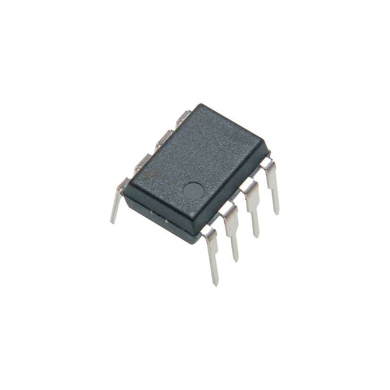
TLC555ID
Standard Timer Single -40°C 85°C 8-Pin SOIC Tube
| Quantity | Unit Price(USD) | Ext. Price |
|---|---|---|
| 1 | $0.805 | $0.80 |
| 10 | $0.713 | $7.13 |
| 30 | $0.626 | $18.78 |
| 100 | $0.561 | $56.10 |
| 500 | $0.535 | $267.50 |
| 1000 | $0.521 | $521.00 |
Inventory:9,834
- 90-day after-sales guarantee
- 365 Days Quality Guarantee
- Genuine Product Guarantee
- 7*24 hours service quarantee
-
Part Number : TLC555ID
-
Package/Case : SOIC-8
-
Brands : TI
-
Components Categories : Programmable Timers and Oscillators
-
Datesheet : TLC555ID DataSheet (PDF)
Overview of TLC555ID
The TLC555 is a monolithic timing circuit fabricated using the TI LinCMOS™ process. The timer is fully compatible with CMOS, TTL, and MOS logic and operates at frequencies up to 2 MHz. Because of its high input impedance, this device supports smaller timing capacitors than those supported by the NE555 or LM555. As a result, more accurate time delays and oscillations are possible. Power consumption is low across the full range of power-supply voltage.
Like the NE555, the TLC555 has a trigger level equal to approximately one-third of the supply voltage and a threshold level equal to approximately two-thirds of the supply voltage. These levels can be altered by use of the control voltage terminal (CONT). When the trigger input (TRIG) falls below the trigger level, the flip-flop is set and the output goes high. If TRIG is above the trigger level and the threshold input (THRES) is above the threshold level, the flip-flop is reset and the output is low. The reset input (RESET) can override all other inputs and can be used to initiate a new timing cycle. If RESET is low, the flip-flop is reset and the output is low. Whenever the output is low, a low-impedance path is provided between the discharge terminal (DISCH) and GND. All unused inputs must be tied to an appropriate logic level to prevent false triggering.
Key Features
- Very low power consumption:
- 1-mW typical at VDD = 5 V
- Capable of operation in astable mode
- CMOS output capable of swinging rail to rail
- High output current capability
- Sink: 100-mA typical
- Source: 10-mA typical
- Output fully compatible with CMOS, TTL, and MOS
- Low supply current reduces spikes during output transitions
- Single-supply operation from 2 V to 15 V
- Functionally interchangeable with the NE555; has same pinout
- ESD protection exceeds 2000 V per MIL-STD-883C, method 3015.2
- Available in Q-temp automotive
- High-reliability automotive applications
- Configuration control and print support
- Qualification to automotive standards
Specifications
The followings are basic parameters of the part selected concerning the characteristics of the part and categories it belongs to.
| Function | General-purpose timer | Iq (typ) (mA) | 0.25 |
| Rating | Catalog | Operating temperature range (°C) | -40 to 125, -40 to 85, 0 to 70 |
| Supply voltage (max) (V) | 15 | Supply voltage (min) (V) | 2 |
Warranty & Returns
Warranty, Returns, and Additional Information
-
QA & Return Policy
Parts Quality Guarantee: 365 days
Returns for refund: within 90 days
Returns for Exchange: within 90 days
-
Shipping and Package
Shipping:For example, FedEx, SF, UPS, or DHL.UPS, or DHL.
Parts Packaging Guarantee: Featuring 100% ESD anti-static protection, our packaging incorporates high toughness and superior buffering capabilities.
-
Payment
For example, channels like VISA, MasterCard, UnionPay, Western Union, PayPal, and more.
If you have specific payment channel preferences or requirements, please get in touch with our sales team for assistance.
Similar Product
TLC555IP
1-MHz, low-power timer, 250-µA, TLC555IP
TLC555CD
Standard Timer Single 0°C 70°C 8-Pin SOIC Tube
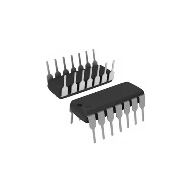
TLC556IN
Standard Timer Dual -40°C 85°C 14-Pin PDIP Tube
TLC2933IPW
Phase Locked Loops - PLL Phase Locked Loop
TLC2933AIPW
Phase Locked Loops - PLL PHASE LOCKED LOOP
TPS3431SDRBR
8-SON -40 to 125

CDCV304PW
The CDCV304PW is a high-performance clock buffer and frequency divider chip designed for use in telecommunications and networking systems

CDCLVC1104PWR
8-pin TSSOP package