

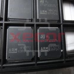
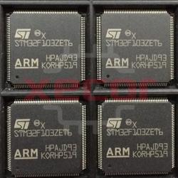
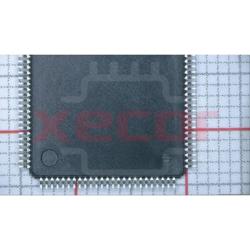
STM32F103C8T6
Microcontroller Unit with 64KB memory
| Quantity | Unit Price(USD) | Ext. Price |
|---|---|---|
| 1 | $1.381 | $1.38 |
| 10 | $1.220 | $12.20 |
| 30 | $1.105 | $33.15 |
| 250 | $1.000 | $250.00 |
| 500 | $0.953 | $476.50 |
| 1000 | $0.932 | $932.00 |
Inventory:8,192
- 90-day after-sales guarantee
- 365 Days Quality Guarantee
- Genuine Product Guarantee
- 7*24 hours service quarantee
-
Part Number : STM32F103C8T6
-
Package/Case : LQFP 48 7x7x1.4 mm
-
Brands : ST
-
Components Categories : Microcontrollers
-
Datesheet : STM32F103C8T6 DataSheet (PDF)
Overview of STM32F103C8T6
The STM32F103C8T6 is a high-performance ARM Cortex-M3 microcontroller from STMicroelectronics. It features a wide range of peripherals and interfaces, making it suitable for a variety of applications including industrial control, consumer electronics, and automotive systems. The STM32F103C8T6 offers high performance, low power consumption, and a rich set of features that make it an ideal choice for embedded applications.
Pinout
(Note: The pin configuration below is a general representation. Refer to the specific datasheet for precise details.)
- Pin 1 (BOOT0): Boot mode selection
- Pin 2 (PC13 / TAMP / SW): General-purpose I/O or tamper or low-power RTC clock calibration output or debugging support
- Pin 3 (PC14 / OSC32_IN): 32.768 kHz crystal oscillator input
- Pin 4 (PC15 / OSC32_OUT): 32.768 kHz crystal oscillator output
- Pin 5 (NRST): External reset input
- Pin 6 (PA0 / WKUP): General-purpose I/O or wakeup (exti_line16)
- Pin 7 (PA1 / ADC12_IN1 / ADC1_IN1): General-purpose I/O or analog to digital converter channel 1 input or analog to digital converter 1 channel 1 input
- Pin 8 (PA2 / ADC12_IN2 / ADC1_IN2): General-purpose I/O or analog to digital converter channel 2 input or analog to digital converter 1 channel 2 input
- Pin 9 (PA3 / ADC12_IN3 / ADC1_IN3): General-purpose I/O or analog to digital converter channel 3 input or analog to digital converter 1 channel 3 input
- Pin 10 (PA4 / ADC12_IN4 / ADC1_IN4): General-purpose I/O or analog to digital converter channel 4 input or analog to digital converter 1 channel 4 input
- Pin 11 (PA5 / ADC12_IN5 / ADC1_IN5): General-purpose I/O or analog to digital converter channel 5 input or analog to digital converter 1 channel 5 input
- Pin 12 (PA6 / ADC12_IN6 / ADC1_IN6): General-purpose I/O or analog to digital converter channel 6 input or analog to digital converter 1 channel 6 input
- Pin 13 (PA7 / ADC12_IN7 / ADC1_IN7): General-purpose I/O or analog to digital converter channel 7 input or analog to digital converter 1 channel 7 input
- Pin 14 (PB0 / ADC12_IN8 / ADC1_IN8): General-purpose I/O or analog to digital converter channel 8 input or analog to digital converter 1 channel 8 input
- Pin 15 (PB1 / ADC12_IN9 / ADC1_IN9): General-purpose I/O or analog to digital converter channel 9 input or analog to digital converter 1 channel 9 input
- Pin 16 (VSS): Ground
- Pin 17 (VDD): Power supply
- Pin 18 (PA8 / CLK_IN / MCO): General-purpose I/O or external clock input or microcontroller clock output
- Pin 19 (PA9 / USART1_TX): General-purpose I/O or USART1 transmitter output
- Pin 20 (PA10 / USART1_RX): General-purpose I/O or USART1 receiver input
- Pin 21 (PA11 / USART1_CTS): General-purpose I/O or USART1 clear to send input
- Pin 22 (PA12 / USART1_RTS): General-purpose I/O or USART1 request to send output
- Pin 23 (PA13 / JTMS / SWDIO): General-purpose I/O or JTAG test mode select or serial wire debug data input/output
- Pin 24 (PA14 / JTCK / SWCLK): General-purpose I/O or JTAG test clock or serial wire debug clock input
- Pin 25 (PA15 / JTDI): General-purpose I/O or JTAG test data input
- Pin 26 (PB3 / JTDO / SWO): General-purpose I/O or JTAG test data output or serial wire debug trace
- Pin 27 (PB4 / JNTRST): General-purpose I/O or JTAG not reset output
- Pin 28 (PB5): General-purpose I/O
- Pin 29 (PB6 / I2C1_SCL): General-purpose I/O or I2C1 clock
- Pin 30 (PB7 / I2C1_SDA): General-purpose I/O or I2C1 data
- Pin 31 (VSSA): Analog ground
- Pin 32 (VDDA): Analog power supply
- Pin 33 (PB8 / CAN1_RX): General-purpose I/O or CAN1 receiver input
- Pin 34 (PB9 / CAN1_TX): General-purpose I/O or CAN1 transmitter output
- Pin 35 (PB10 / USART3_TX): General-purpose I/O or USART3 transmitter output
- Pin 36 (PB11 / USART3_RX): General-purpose I/O or USART3 receiver input
- Pin 37 (VSS): Ground
- Pin 38 (VDD): Power supply
- Pin 39 (PB12 / SPI2_NSS): General-purpose I/O or SPI2 slave select input
- Pin 40 (PB13 / SPI2_SCK): General-purpose I/O or SPI2 serial clock input
- Pin 41 (PB14 / SPI2_MISO): General-purpose I/O or SPI2 master in slave out input
- Pin 42 (PB15 / SPI2_MOSI): General-purpose I/O or SPI2 master out slave in output
- Pin 43 (PC6 / TIM3_CH1): General-purpose I/O or timer 3 channel 1 input/output
- Pin 44 (PC7 / TIM3_CH2): General-purpose I/O or timer 3 channel 2 input/output
- Pin 45 (PC8 / TIM3_CH3): General-purpose I/O or timer 3 channel 3 input/output
- Pin 46 (PC9 / TIM3_CH4): General-purpose I/O or timer 3 channel 4 input/output
- Pin 47 (VSS): Ground
- Pin 48 (VDD): Power supply
Circuit Diagram
Include a circuit diagram that illustrates the connections and operation of the STM32F103C8T6 for a visual representation.
Key Features
- ARM Cortex-M3 Core: The STM32F103C8T6 is based on the ARM Cortex-M3 core, providing high performance and efficient processing.
- Flash Memory: The microcontroller features 64KB of flash memory for program storage.
- SRAM: It includes 20KB of SRAM for data storage.
- Peripherals: The STM32F103C8T6 features a variety of peripherals including UART, SPI, I2C, ADC, and PWM channels.
- Low Power Consumption: The microcontroller is designed for low power consumption, making it suitable for battery-powered applications.
Note: For detailed technical specifications, refer to the STM32F103C8T6 datasheet.
Application
- Industrial Control: The STM32F103C8T6 is suitable for use in industrial control systems for monitoring and control applications.
- Consumer Electronics: It can be used in consumer electronics such as smart home devices and wearable technology.
- Automotive Systems: Ideal for automotive applications requiring embedded control and monitoring.
Functionality
The STM32F103C8T6 provides a convenient and reliable solution for embedded applications, offering high performance and a rich set of features.
Power Supply: Connect VDD and VDDA pins to the supply voltage and connect VSS pins to ground. GPIO Pins: Use the GPIO pins for general purpose input/output operations. Peripheral Interfaces: Utilize the UART, SPI, I2C, ADC, and PWM channels for various interfacing requirements.
Usage Guide:
- Power Supply: Connect VDD and VDDA pins to the supply voltage and connect VSS pins to ground.
- GPIO Pins: Use the GPIO pins for general purpose input/output operations.
- Peripheral Interfaces: Utilize the UART, SPI, I2C, ADC, and PWM channels for various interfacing requirements.
Frequently Asked Questions
Q: What is the maximum clock frequency of the STM32F103C8T6?
A: The maximum clock frequency of the STM32F103C8T6 is specified in the datasheet and depends on the operating conditions.
Q: Can the STM32F103C8T6 operate in low power modes?
A: Yes, the STM32F103C8T6 features low power modes for minimizing power consumption in battery-powered applications.
Specifications
The followings are basic parameters of the part selected concerning the characteristics of the part and categories it belongs to.
| Operating Range | Industrial | Supply Voltage Min Volt | 2.0 |
| Supply Voltage Max Volt | 3.6 | Operating Temp Min Celsius | -40.0 |
| Operating Temp Max Celsius | 85.0 | Core | Arm Cortex-M3 |
| ECCN US | 3A991.a.2 | ECCN EU | NEC |
| Packing Type | Tray | RoHs compliant | Ecopack2 |
| Grade | Industrial | Package Name | LQFP 48 7x7x1.4 mm |
Equivalent Parts
The followings are basic parameters of the part selected concerning the characteristics of the part and categories it belongs to.
STM32F103C8T6 Equivalent Parts
For the STM32F103C8T6 component, you may consider these replacement and alterative parts.
| Models | Manufacturer | Package/Case | Description |
|---|---|---|---|
| STM32F103C6T6 | Stmicroelectronics | LQFP-48 | ARM? Cortex?-M3 STM32F1 Microcontroller IC 32-Bit Single-Core 72MHz 32KB (32K x 8) FLASH |
| STM32F103CBT6 | Stmicroelectronics | LQFP-48 | A similar microcontroller with additional features and peripherals. |
| STM32F103RET6 | Stmicroelectronics | LQFP64 | Another alternative offering enhanced performance and memory capacity. |
Warranty & Returns
Warranty, Returns, and Additional Information
-
QA & Return Policy
Parts Quality Guarantee: 365 days
Returns for refund: within 90 days
Returns for Exchange: within 90 days
-
Shipping and Package
Shipping:For example, FedEx, SF, UPS, or DHL.UPS, or DHL.
Parts Packaging Guarantee: Featuring 100% ESD anti-static protection, our packaging incorporates high toughness and superior buffering capabilities.
-
Payment
For example, channels like VISA, MasterCard, UnionPay, Western Union, PayPal, and more.
If you have specific payment channel preferences or requirements, please get in touch with our sales team for assistance.
Similar Product

STM32F446RET6
Medical 64-Pin LQFP

STM32F407VGT6
High-performance foundation line
STM32F103ZGT6
Ideal for mainstream applications requiring reliable performance
STM32F103ZET6
With its advanced features and robust design
STM32F103VCT6
MCU 32-bit STM32F1 ARM Cortex M3 RISC 256KB Flash 2.5V/3.3V 100-Pin LQFP Tray
STM32F091VCT6
Tray-packaged STM32F091VCT6 with 256KB Flash memory and support for 2.5V/3.3V operation
STM32F405RGT6
Arm Cortex-M4 core with DSP and FPU for efficient processing

STM32L476VGT6
1.71V~3.6V operating voltage