
SST39VF040-70-4C-NHE
NOR Flash Parallel 3.3V 4M-bit 512K x 8 70ns 32-Pin PLCC Tube
Inventory:7,982
- 90-day after-sales guarantee
- 365 Days Quality Guarantee
- Genuine Product Guarantee
- 7*24 hours service quarantee
-
Part Number : SST39VF040-70-4C-NHE
-
Package/Case : PLCC-32
-
Brands : MICROCHIP
-
Components Categories : Memory
-
Datesheet : SST39VF040-70-4C-NHE DataSheet (PDF)
Overview of SST39VF040-70-4C-NHE
The SST39VF040-70-4C-NHE is a top-of-the-line flash memory device that boasts a whopping 5124K x8CMOS capacity. Utilizing innovative CMOS SuperFlash technology developed by SST, this device offers unparalleled performance and reliability. With a unique split-gate cell design and thick-oxide tunneling injector, the SST39VF040 ensures seamless read and write operations, outperforming its competitors in both reliability and manufacturability. Operating on a modest 2.7-3.6V power supply, this flash memory device is energy-efficient and cost-effective. The device also adheres to industry standards, making it compatible with JEDEC standard pinouts for x8 memories
Key Features
- Organized as 64K x8 / 128K x8 / 256K x8 / 512K x8
- Single Voltage Read and Write Operations– 3.0-3.6V for SST39LF512/010/020/040– 2.7-3.6V for SST39VF512/010/020/040
- Superior Reliability– Endurance: 100,000 Cycles (typical)– Greater than 100 years Data Retention
- Low Power Consumption(typical values at 14 MHz)– Active Current: 5 mA (typical)– Standby Current: 1 µA (typical)
- Sector-Erase Capability– Uniform 4 KByte sectors
- Fast Read Access Time:– 45 ns for SST39LF512/010/020/040– 55 ns for SST39LF020/040– 70 ns for SST39VF512/010/020/040
- Latched Address and Data
- Fast Erase and Byte-Program:– Sector-Erase Time: 18 ms (typical)– Chip-Erase Time: 70 ms (typical)– Byte-Program Time: 14 µs (typical)– Chip Rewrite Time:1 second (typical) for SST39LF/VF5122 seconds (typical) for SST39LF/VF0104 seconds (typical) for SST39LF/VF0208 seconds (typical) for SST39LF/VF040
- Automatic Write Timing– Internal VPP Generation
- End-of-Write Detection– Toggle Bit– Data# Polling
- CMOS I/O Compatibility
- JEDEC Standard– Flash EEPROM Pinouts and command sets
- Packages Available– 32-lead PLCC– 32-lead TSOP (8mm x 14mm)– 48-ball TFBGA (6mm x 8mm)– 34-ball WFBGA (4mm x 6mm) for 1M and 2M
- All devices are RoHS compliant
Specifications
The followings are basic parameters of the part selected concerning the characteristics of the part and categories it belongs to.
| Product Category | NOR Flash | RoHS | Details |
| Mounting Style | SMD/SMT | Package / Case | PLCC-32 |
| Series | SST39VF | Memory Size | 4 Mbit |
| Supply Voltage - Min | 2.7 V | Supply Voltage - Max | 3.6 V |
| Active Read Current - Max | 20 mA | Interface Type | Parallel |
| Organization | 512 k x 8 | Data Bus Width | 8 bit |
| Timing Type | Asynchronous | Minimum Operating Temperature | 0 C |
| Maximum Operating Temperature | + 70 C | Architecture | Sector |
| Brand | Microchip Technology | Memory Type | NOR |
| Moisture Sensitive | Yes | Product Type | NOR Flash |
| Speed | 70 ns | Standard | Not Supported |
| Factory Pack Quantity | 30 | Subcategory | Memory & Data Storage |
| Unit Weight | 0.082306 oz |
Warranty & Returns
Warranty, Returns, and Additional Information
-
QA & Return Policy
Parts Quality Guarantee: 365 days
Returns for refund: within 90 days
Returns for Exchange: within 90 days
-
Shipping and Package
Shipping:For example, FedEx, SF, UPS, or DHL.UPS, or DHL.
Parts Packaging Guarantee: Featuring 100% ESD anti-static protection, our packaging incorporates high toughness and superior buffering capabilities.
-
Payment
For example, channels like VISA, MasterCard, UnionPay, Western Union, PayPal, and more.
If you have specific payment channel preferences or requirements, please get in touch with our sales team for assistance.
Similar Product

AT26DF081A-SSU
NOR Flash 8M, 2.7V, 70Mhz Serial Flash

SST25VF010A-33-4C-SAE
Flash Serial-SPI 3.3V 1Mbit 128K x 8bit 12ns 8-Pin SOIC N Tube
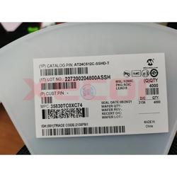
AT24C512C-SSHD-T
Capacity: 512KB
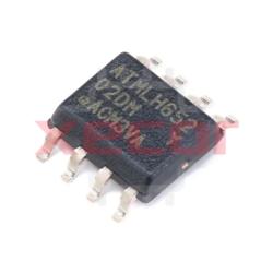
AT24C02D-SSHM-T
IC EEPROM with capacity of 2KBIT and operating frequency of 1MHZ in 8SOIC package
AT25640B-SSHL-T
This product is an EEPROM with a 64K density and SPI interface
SST25VF032B-80-4I-QAE
NOR Flash 32M (4Mx8) 80MHz Industrial Temp
AT24C512C-SSHM-T
Small form factor memory chip
AT24C256C-SSHL-B
Small-sized serial EEPROM