
SN74LVCH8T245RHLR
Voltage Level Translator 8-CH Bidirectional 24-Pin VQFN EP T/R
Inventory:8,282
- 90-day after-sales guarantee
- 365 Days Quality Guarantee
- Genuine Product Guarantee
- 7*24 hours service quarantee
-
Part Number : SN74LVCH8T245RHLR
-
Package/Case : QFN-24
-
Brands : TI
-
Components Categories : Buffers, Drivers, Receivers, Transceivers
-
Datesheet : SN74LVCH8T245RHLR DataSheet (PDF)
Overview of SN74LVCH8T245RHLR
The SN74LVCH8T245 is an 8-bit noninverting bus transceiver that uses two separate configurable power-supply rails. The A port is designed to track VCCA, which accepts any supply voltage from 1.65 V to 5.5 V. The B port is designed to track VCCB, which also accepts any supply voltage from 1.65 V to 5.5 V. This allows for universal low-voltage bidirectional translation between any of the 1.8-V, 2.5-V, 3.3-V, and 5.5-V voltage nodes.
The SN74LVCH8T245 is designed for asynchronous communication between two data buses. The logic levels of the direction-control (DIR) input and the output-enable (OE) input activate either the B-port outputs, the A-port outputs, or place both output ports into a high-impedance state. The device transmits data from the A bus to the B bus when the B-port outputs are activated, and from the B bus to the A bus when the A-port outputs are activated. The input circuitry on both A and B ports are always active.
Active bus-hold circuitry holds unused or undriven inputs at a valid logic state. Use of pullup or pulldown resistors with the bus-hold circuitry is not recommended. This device is fully specified for partial-power-down applications using Ioff. The Ioff circuitry disables the outputs, preventing damaging current backflow through the device. The VCC isolation feature ensures that if either VCCA or VCCB is at GND, then the outputs are in the high-impedance state. To ensure the high-impedance state during power up or power down, OE should be tied to VCCA through a pullup resistor; the minimum value of the resistor is determined by the current-sinking capability of the driver.
The SN74LVCH8T245 is designed so that the control pins (DIR and OE) are referenced to VCCA.
Key Features
- Control inputs (DIR and OE) VIH and VIL levels are referenced to VCCA
- Bus hold on data inputs eliminates the need for external pullup and pulldown resistors
- VCC isolation
- Fully configurable dual-rail design
- Ioff supports Partial-Power-Down node operation
- Latch-up performance exceeds 100 mA per JESD 78, class II
- ESD protection exceeds JESD 22
Specifications
The followings are basic parameters of the part selected concerning the characteristics of the part and categories it belongs to.
| Technology family | LVC | Bits (#) | 8 |
| High input voltage (min) (V) | 1.08 | High input voltage (max) (V) | 5.5 |
| Vout (min) (V) | 1.65 | Vout (max) (V) | 5.5 |
| Data rate (max) (MBps) | 200 | IOH (max) (mA) | -32 |
| IOL (max) (mA) | 32 | Supply current (max) (µA) | 25 |
| Features | Bus-hold, Output enable, Overvoltage tolerant inputs, Partial power down (Ioff), Vcc isolation | Input type | Bidirectional, CMOS, Overvoltage Tolerant |
| Output type | 3-State, Balanced CMOS, Push-Pull | Rating | Catalog |
| Operating temperature range (°C) | -40 to 85 |
Warranty & Returns
Warranty, Returns, and Additional Information
-
QA & Return Policy
Parts Quality Guarantee: 365 days
Returns for refund: within 90 days
Returns for Exchange: within 90 days
-
Shipping and Package
Shipping:For example, FedEx, SF, UPS, or DHL.UPS, or DHL.
Parts Packaging Guarantee: Featuring 100% ESD anti-static protection, our packaging incorporates high toughness and superior buffering capabilities.
-
Payment
For example, channels like VISA, MasterCard, UnionPay, Western Union, PayPal, and more.
If you have specific payment channel preferences or requirements, please get in touch with our sales team for assistance.
Similar Product
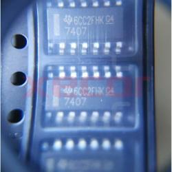
SN7407DR
High-voltage open-collector output configuration
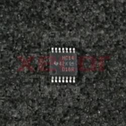
SN74HC14PWR
Inverter Schmitt Trigger 6-Element CMOS 14-Pin TSSOP T/R
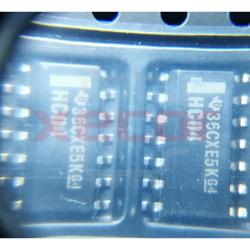
SN74HC04DR
Inverter 6-Element CMOS Automotive 14-Pin SOIC T/R

SN5404J
Contains 6 inverters with a voltage range of 4.5V to 5.5V

SN74AHC14PWR
Inverter Schmitt Trigger 6-Element CMOS 14-Pin TSSOP T/R
SN74LVC1G06DCKR
Buffer/Driver 1-CH Inverting Open Drain CMOS 5-Pin SC-70 T/R
SN74LVC1G32DCKR
Positive logic gates with dual inputs

SN74LVC1G126DCKR
Buffer/Line Driver 1-CH Non-Inverting 3-ST CMOS 5-Pin SC-70 T/R