
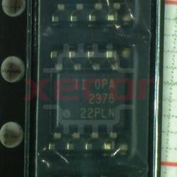
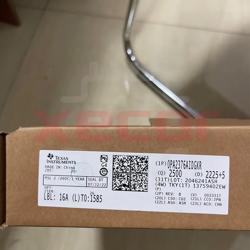
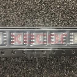
OPA317IDBVR
Operational Amplifiers - Op Amps Low Offset,RRIO Op Amp
| Quantity | Unit Price(USD) | Ext. Price |
|---|---|---|
| 1 | $0.539 | $0.54 |
| 10 | $0.447 | $4.47 |
| 30 | $0.400 | $12.00 |
| 100 | $0.354 | $35.40 |
| 500 | $0.327 | $163.50 |
| 1000 | $0.312 | $312.00 |
Inventory:5,367
- 90-day after-sales guarantee
- 365 Days Quality Guarantee
- Genuine Product Guarantee
- 7*24 hours service quarantee
-
Part Number : OPA317IDBVR
-
Package/Case : SOT23-5
-
Brands : TI
-
Components Categories : AmplifiersInstrumentation, OP Amps, Buffer Amps
-
Datesheet : OPA317IDBVR DataSheet (PDF)
Overview of OPA317IDBVR
The OPA317 series of CMOS operational amplifiers offer precision performance at a very competitive price. These devices are members of the Zerø-Drift family of amplifiers that use a proprietary autocalibration technique to simultaneously provide low offset voltage (90 µV maximum) and near-zero drift over time and temperature at only 35 µA (maximum) of quiescent current.
The OPA317 family features rail-to-rail input and output in addition to near flat 1/f noise, making this amplifier ideal for many applications, and much easier to design into a system. These devices are optimized for low-voltage operation as low as 1.8 V (\xC2±0.9 V) and up to 5.5 V (±2.75 V).
The OPA317 (single version) is available in the SC70-5, SOT23-5, and SOIC-8 packages. The OPA2317 (dual version) is offered in the VSSOP-8 and SOIC-8 packages. The OPA4317 is offered in the standard SOIC-14 and TSSOP-14 packages. All versions are specified for operation from 40°C to 125°C.
Key Features
- Supply Voltage: 1.8 V to 5.5 V
- microPackages:
- Single: SOT23-5, SC-70, SOIC-8
- Dual: VSSOP-8, SOIC-8
- Quad: SOIC-14, TSSOP-14
- Low Offset Voltage: 20 µV (Typical)
- CMRR: 108-dB (Typical) PSRR
- Quiescent Current: 35 µA (Maximum)
- Gain Bandwidth: 300 kHz
- Rail-to-Rail Input and Output
- Internal EMI and RFI Filtering
Specifications
The followings are basic parameters of the part selected concerning the characteristics of the part and categories it belongs to.
| Number of channels | 1 | Total supply voltage (+5 V = 5, ±5 V = 10) (max) (V) | 5.5 |
| Total supply voltage (+5 V = 5, ±5 V = 10) (min) (V) | 1.8 | Vos (offset voltage at 25°C) (max) (mV) | 0.09 |
| GBW (typ) (MHz) | 0.3 | Features | EMI Hardened, Small Size, Zero Drift |
| Slew rate (typ) (V/µs) | 0.15 | Rail-to-rail | In, Out |
| Offset drift (typ) (µV/°C) | 0.05 | Iq per channel (typ) (mA) | 0.021 |
| Vn at 1 kHz (typ) (nV√Hz) | 55 | CMRR (typ) (dB) | 108 |
| Rating | Catalog | Operating temperature range (°C) | -40 to 125 |
| Iout (typ) (A) | 0.005 | Architecture | CMOS |
| Input common mode headroom (to negative supply) (typ) (V) | -0.1 | Input common mode headroom (to positive supply) (typ) (V) | 0.1 |
| Output swing headroom (to negative supply) (typ) (V) | 0.03 | Output swing headroom (to positive supply) (typ) (V) | -0.03 |
Warranty & Returns
Warranty, Returns, and Additional Information
-
QA & Return Policy
Parts Quality Guarantee: 365 days
Returns for refund: within 90 days
Returns for Exchange: within 90 days
-
Shipping and Package
Shipping:For example, FedEx, SF, UPS, or DHL.UPS, or DHL.
Parts Packaging Guarantee: Featuring 100% ESD anti-static protection, our packaging incorporates high toughness and superior buffering capabilities.
-
Payment
For example, channels like VISA, MasterCard, UnionPay, Western Union, PayPal, and more.
If you have specific payment channel preferences or requirements, please get in touch with our sales team for assistance.
Similar Product

OPA376AIDBVR
High-performance operational amplifier
OPA2376AIDR
Dual operational amplifier offering precision, low noise performance, and low quiescent current
OPA2376AIDGKR
High-precision, low-noise dual operational amplifier with low quiescent current, designed for applications requiring accuracy and efficiency

OPA404KP
Quad operational
OPA541AP
Single TO-220-11 package for ease of installation
OPA627AP
Superior performance for demanding applications
LMC6482AIM/NOPB
SMD Integrated Circuit
OPA2330AIDR
OPA2330AIDR is an op amp that contains two general-purpose channels, capable of operation within a voltage range of ±2