
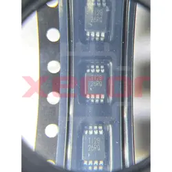
OPA2991QDGKRQ1
Op Amp Dual Low Noise Amplifier R-R I/O ±20V/40V Automotive 8-Pin VSSOP T/R
Inventory:8,218
- 90-day after-sales guarantee
- 365 Days Quality Guarantee
- Genuine Product Guarantee
- 7*24 hours service quarantee
-
Part Number : OPA2991QDGKRQ1
-
Package/Case : VSSOP-8
-
Brands : TI
-
Components Categories : General-purpose op amps
-
Datesheet : OPA2991QDGKRQ1 DataSheet (PDF)
Overview of OPA2991QDGKRQ1
The OPAx991-Q1 family (OPA991-Q1, OPA2991-Q1, and OPA4991-Q1) is a family of high voltage (40 V) general purpose operational amplifiers for automotive application. These devices offer exceptional DC precision and AC performance, including rail-to-rail input or output, low offset (±125 µV, typical), low offset drift (±0.3 µV/°C, typical), low noise (10.8 nV/√ Hz and 1.8 µV PP), and 4.5-MHz bandwidth.
Unique features such as differential and common-mode input-voltage range to the supply rail, high output current (±75 mA), high slew rate (21 V/µs), and high capacitive load drive (1 nF) make the OPAx991-Q1 a robust, high-performance operational amplifier for high-voltage automotive applications.
The OPAx991-Q1 family of op amps is available in standard packages (such as SOT-23, SOIC, VSSOP, and TSSOP) and is specified from –40°C to 125°C.
Key Features
- AEC-Q100 qualified for automotive applications
- Temperature grade 1: –40°C to +125°C, T A
- Device HBM ESD classification level 2A
- Device CDM ESD classification level C6
- Low offset voltage: ±125 µV
- Low offset voltage drift: ±0.3 µV/°C
- Low noise: 10.8 nV/√ Hz at 1 kHz
- High common-mode rejection: 130 dB
- Low bias current: ±10 pA
- Rail-to-rail input and output
- Wide bandwidth: 4.5 MHz GBW
- High slew rate: 21 V/µs
- High capacitive load drive: 1 nF
- MUX-friendly/comparator inputs
- Amplifier operates with differential inputs up to supply rail
- Amplifier can be used in open-loop or as comparator
- Low quiescent current: 560 µA per amplifier
- Wide supply: ±1.35 V to ±20 V, 2.7 V to 40 V
- Robust EMIRR performance: EMI/RFI filters on input and supply pins
Specifications
The followings are basic parameters of the part selected concerning the characteristics of the part and categories it belongs to.
| Number of channels | 2 | Total supply voltage (+5 V = 5, ±5 V = 10) (max) (V) | 40 |
| Total supply voltage (+5 V = 5, ±5 V = 10) (min) (V) | 2.7 | Rail-to-rail | In, Out |
| GBW (typ) (MHz) | 4.5 | Slew rate (typ) (V/µs) | 21 |
| Vos (offset voltage at 25°C) (max) (mV) | 0.895 | Iq per channel (typ) (mA) | 0.56 |
| Vn at 1 kHz (typ) (nV√Hz) | 10.8 | Rating | Automotive |
| Operating temperature range (°C) | -40 to 125 | Offset drift (typ) (µV/°C) | 0.3 |
| Features | EMI Hardened, High Cload Drive, MUX Friendly | CMRR (typ) (dB) | 130 |
| Iout (typ) (A) | 0.075 | Architecture | CMOS |
| Input common mode headroom (to negative supply) (typ) (V) | -0.1 | Input common mode headroom (to positive supply) (typ) (V) | 0.1 |
| Output swing headroom (to negative supply) (typ) (V) | 0.025 | Output swing headroom (to positive supply) (typ) (V) | -0.025 |
Warranty & Returns
Warranty, Returns, and Additional Information
-
QA & Return Policy
Parts Quality Guarantee: 365 days
Returns for refund: within 90 days
Returns for Exchange: within 90 days
-
Shipping and Package
Shipping:For example, FedEx, SF, UPS, or DHL.UPS, or DHL.
Parts Packaging Guarantee: Featuring 100% ESD anti-static protection, our packaging incorporates high toughness and superior buffering capabilities.
-
Payment
For example, channels like VISA, MasterCard, UnionPay, Western Union, PayPal, and more.
If you have specific payment channel preferences or requirements, please get in touch with our sales team for assistance.
Similar Product
OPA350UA
rail-to-rail single operational amplifier for single-supply applications
OPA227U
With advanced technology and superior design, the OPA227U delivers unmatched accuracy and minimal background noise

OPA1632DGN
channel audio amplifier IC OPA1632DGN in HVSSOP8 package supports power supply voltages between 5VDC and 30VDC
OPA2209AIDGKT
Dual Operational Amplifier with Low Noise Performance and Rail-to-Rail Output Capability at ±18V/36V

OPA2277U/2K5
1MHz Bandwidth Operational Amplifier General Purpose in 8-SOIC IC
OPA2182IDGKR
Operational Amplifiers - Op Amps Industry’s lowest offset drift (0.012 uV/°C, max), 5.7 nV/rtHz, MUX-friendly 36V op amp 8-VSSOP -40 to 125
OPA2192IDR
Op Amp Dual Precision Amplifier R-R I/O ±18V/36V 8-Pin SOIC T/R
OPA2187IDR
Operational Amplifiers - Op Amps 1AuV Vos, 0.005AuV/A C Low-Power 36V