
NJG1681MD7
RF Switch ICs High Power SPDT Switch GaAs MMIC
Inventory:6,013
- 90-day after-sales guarantee
- 365 Days Quality Guarantee
- Genuine Product Guarantee
- 7*24 hours service quarantee
-
Part Number : NJG1681MD7
-
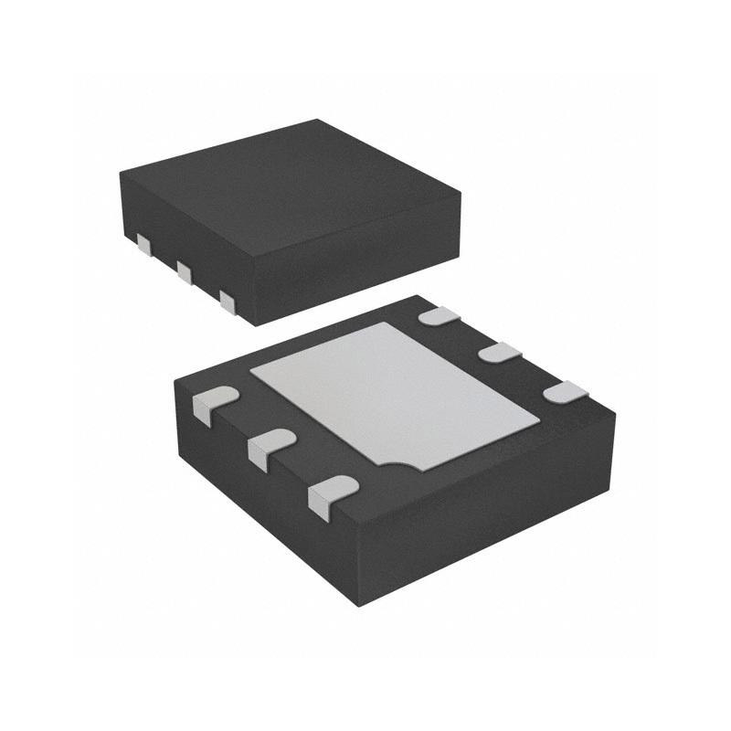
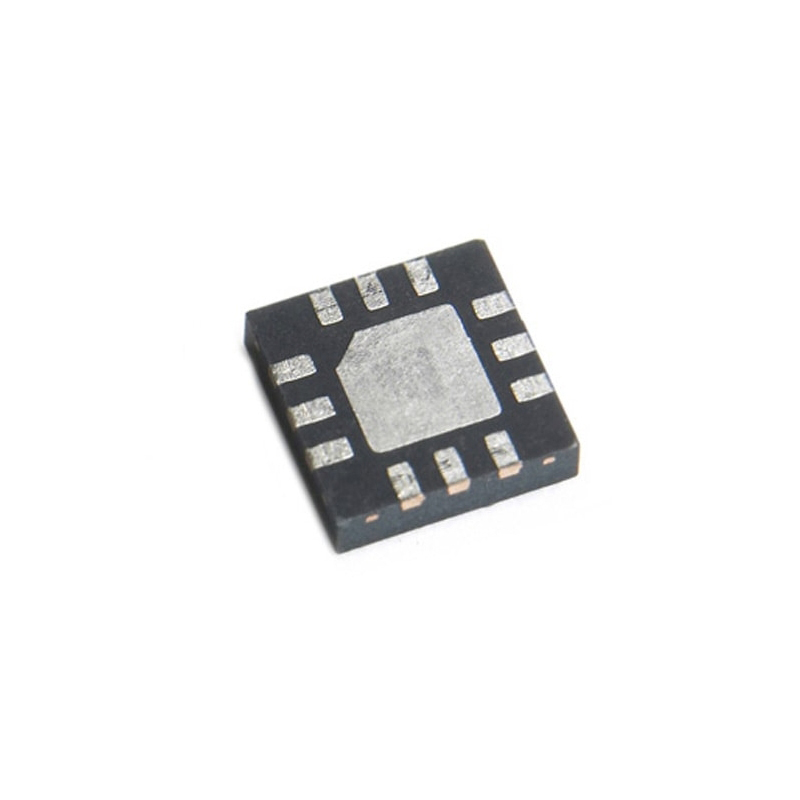
Package/Case : QFN-14
-
Brands : nisshinbo micro devices
-
Components Categories : RF Switches
-
Datesheet : NJG1681MD7 DataSheet (PDF)
Overview of NJG1681MD7
The NJG1681MD7 is a high-performance RF amplifier IC designed for use in a variety of wireless communication applications. It offers low noise figure, high gain, and high linearity, making it ideal for use in cellular base stations, repeaters, and other wireless infrastructure applications.
Pinout
(Note: The pin configuration below is a general representation. Refer to the specific datasheet for precise details.)
- VCC: Power Supply
- GND: Ground
- RF IN: RF Input
- RF OUT: RF Output
- VCTL: Control Voltage
Circuit Diagram
Incorporate a circuit diagram that illustrates the connections and operation of the NJG1681MD7 RF amplifier IC for a more visual representation.
Key Features
- Low Noise Figure: The NJG1681MD7 offers a low noise figure, ensuring minimal signal degradation and high sensitivity in receiver applications.
- High Gain: With high gain, the NJG1681MD7 provides amplification for weak signals, improving the overall performance of the RF system.
- High Linearity: The NJG1681MD7 offers high linearity, reducing signal distortion and improving the quality of transmitted signals.
- Wide Frequency Range: The NJG1681MD7 operates over a wide frequency range, making it suitable for use in various wireless communication systems.
Note: For detailed technical specifications, refer to the NJG1681MD7 datasheet.
Application
- Cellular Base Stations: The NJG1681MD7 is ideal for use in cellular base stations, providing amplification for signals transmitted and received by the base station.
- Repeaters: It can be used in repeaters to amplify and retransmit signals, extending the coverage area of wireless networks.
- Wireless Infrastructure: The NJG1681MD7 is suitable for use in various wireless infrastructure applications, such as Wi-Fi access points and small cells.
- RF Test Equipment: It can be used in RF test equipment to amplify and analyze RF signals.
Functionality
The NJG1681MD7 RF amplifier IC provides high-performance amplification for a wide range of wireless communication applications, offering reliability and efficiency in a compact form factor.
Usage Guide
- Power Supply: Connect VCC (Power Supply Pin) to the appropriate power supply voltage and GND (Ground Pin) to ground.
- RF Interface: Connect the RF IN and RF OUT pins to the RF input and output ports of the system, respectively.
- Control Voltage: Use the VCTL pin to control the gain of the amplifier.
Frequently Asked Questions
-
Q: What is the typical gain of the NJG1681MD7?
- A: The NJG1681MD7 typically has a gain of around 15 dB, providing sufficient amplification for most wireless communication applications.
-
Q: Is the NJG1681MD7 suitable for high-frequency applications?
- A: Yes, the NJG1681MD7 operates over a wide frequency range, making it suitable for high-frequency applications in the GHz range.
Specifications
The followings are basic parameters of the part selected concerning the characteristics of the part and categories it belongs to.
| Product Category | RF Switch ICs | RoHS | Details |
| Switch Configuration | SPDT | Maximum Frequency | 6 GHz |
| Insertion Loss | 0.45 dB | Off Isolation - Typ | 20 dB |
| Minimum Operating Temperature | - 40 C | Maximum Operating Temperature | + 105 C |
| Mounting Style | SMD/SMT | Package / Case | QFN-14 |
| Technology | GaAs | Series | NJG1681 |
| Brand | Nisshinbo | High Control Voltage | 1.8 V |
| Number of Switches | Single | Operating Supply Current | 95 uA |
| Pd - Power Dissipation | 1.3 W | Product Type | RF Switch ICs |
| Factory Pack Quantity | 3000 | Subcategory | Wireless & RF Integrated Circuits |
| Supply Voltage - Max | 5 V | Supply Voltage - Min | 2.375 V |
| Tradename | NJG168 | Unit Weight | 0.001136 oz |
Equivalent Parts
The followings are basic parameters of the part selected concerning the characteristics of the part and categories it belongs to.
NJG1681MD7 Equivalent Parts
For the NJG1681MD7 component, you may consider these replacement and alterative parts.
| Models | Manufacturer | Package/Case | Description |
|---|---|---|---|
| MASW-011094 | MACOM Technology Solutions | QFN and QFN-24 | Another SPDT switch from MACOM with comparable high-power handling capabilities. |
| HMC1121 | Analog Devices | QFN-40 | Another high-power SPDT switch from Analog Devices with similar specifications. |
| PE4259 | pSemi Corporation | QFN and QFN-24 | A high-power SPDT switch from Peregrine Semiconductor with similar specifications. |
Warranty & Returns
Warranty, Returns, and Additional Information
-
QA & Return Policy
Parts Quality Guarantee: 365 days
Returns for refund: within 90 days
Returns for Exchange: within 90 days
-
Shipping and Package
Shipping:For example, FedEx, SF, UPS, or DHL.UPS, or DHL.
Parts Packaging Guarantee: Featuring 100% ESD anti-static protection, our packaging incorporates high toughness and superior buffering capabilities.
-
Payment
For example, channels like VISA, MasterCard, UnionPay, Western Union, PayPal, and more.
If you have specific payment channel preferences or requirements, please get in touch with our sales team for assistance.
Similar Product
NJG1801K75-TE1
RF Switches DFN-6(1x1) ROHS
NJG1681MD7-TE1
RF Switch ICs Ultra Low Pwr Op Amp GaAs MMIC ESD
NJG1817ME4-TE1
Versatile 25dB RF switch with ultra-low insertion loss
NJG1816K75-TE1
ROHS compliant for environmentally friendly usage
NJG1806K75-TE1
Compact DFN6 SMD design for easy surface mounting

NJG1804K64
The NJG1804K64 is a high-performance RF transceiver chip designed for wireless communication applications
NJG1684ME2-TE1
Compact and efficient NJR NJG1684ME2-TE1, RL module
NJG1812ME4-TE1
Experience seamless RF signal switching with NJG1812ME4-TE1's advanced technology