
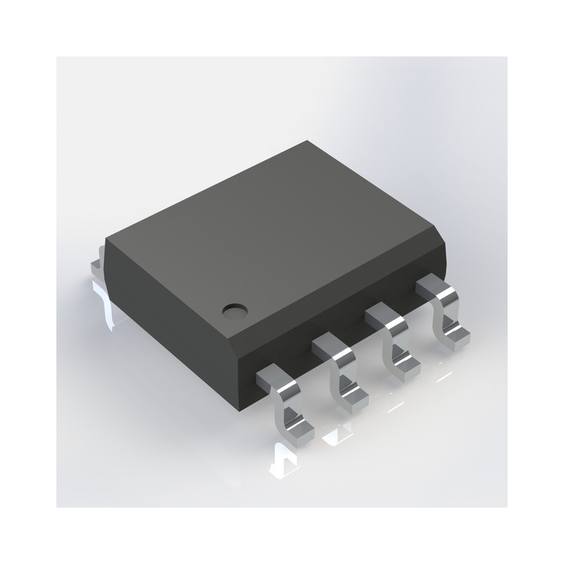
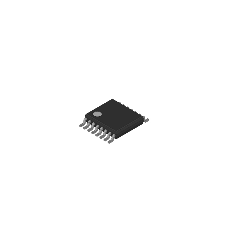
CY2308ZXI-1H
Zero Delay Buffer 8-Out LVCMOS Single-Ended 16-Pin TSSOP Tube
Inventory:7,583
- 90-day after-sales guarantee
- 365 Days Quality Guarantee
- Genuine Product Guarantee
- 7*24 hours service quarantee
-
Part Number : CY2308ZXI-1H
-
Package/Case : TSSOP
-
Brands : Infineon Technologies
-
Components Categories : Clock Generators, PLLs, Frequency Synthesizers
-
Datesheet : CY2308ZXI-1H DataSheet (PDF)
The CY2308ZXI-1H is a high-performance Zero Delay Buffer IC designed for clock distribution applications in electronic systems. This IC features zero input-output propagation delay, making it ideal for synchronizing clock signals in advanced digital designs. (Note: The pin configuration below is a general representation. Refer to the specific datasheet for precise details.) Include a circuit diagram illustrating the connections and operation of the CY2308ZXI-1H IC for a visual representation. Note: For detailed technical specifications, please refer to the CY2308ZXI-1H datasheet. Functionality The CY2308ZXI-1H is a high-performance Zero Delay Buffer IC that ensures synchronized clock signals with zero propagation delay, making it a reliable choice for applications demanding precise timing requirements. Usage Guide Q: What is the purpose of the spread disable pin (SD) in the CY2308ZXI-1H? Q: Can the CY2308ZXI-1H operate with external crystal oscillators? For similar functionalities, consider these alternatives to the CY2308ZXI-1H:Overview of CY2308ZXI-1H
Pinout
Circuit Diagram
Key Features
Application
Frequently Asked Questions
A: The spread disable pin (SD) allows users to disable spread spectrum clocking for applications requiring constant clock frequencies without modulation.
A: Yes, the CY2308ZXI-1H supports crystal oscillators, providing accurate and stable clock signals in systems requiring precise timing references.Equivalent
Specifications
The followings are basic parameters of the part selected concerning the characteristics of the part and categories it belongs to.
| Product Status | Active | Programmabe | Not Verified |
| Type | Zero Delay PLL Clock Buffer | PLL | Yes with Bypass |
| Input | LVCMOS, LVTTL | Output | LVCMOS |
| Ratio - Input:Output | 1:8 | Differential - Input:Output | No/No |
| Frequency - Max | 133.3MHz | Divider/Multiplier | No/No |
| Voltage - Supply | 3V ~ 3.6V | Operating Temperature | -40°C ~ 85°C |
| Mounting Type | Surface Mount | Package / Case | TSSOP-16 |
| Supplier Device Package | 16-TSSOP | Base Product Number | CY2308 |
| Manufacturer | Infineon | Product Category | Clock Buffer |
| RoHS | Details | Series | CY2308ZXI |
| Number of Outputs | 8 Output | Maximum Input Frequency | 133 MHz |
| Supply Voltage - Max | 3.6 V | Supply Voltage - Min | 3 V |
| Propagation Delay - Max | 0 ps | Minimum Operating Temperature | - 40 C |
| Maximum Operating Temperature | + 85 C | Mounting Style | SMD/SMT |
| Brand | Infineon Technologies | Height | 0.95 mm |
| Length | 5.1 mm | Moisture Sensitive | Yes |
| Product Type | Clock Buffers | Factory Pack Quantity | 480 |
| Subcategory | Clock & Timer ICs | Width | 4.5 mm |
| Unit Weight | 0.006102 oz |
Warranty & Returns
Warranty, Returns, and Additional Information
-
QA & Return Policy
Parts Quality Guarantee: 365 days
Returns for refund: within 90 days
Returns for Exchange: within 90 days
-
Shipping and Package
Shipping:For example, FedEx, SF, UPS, or DHL.UPS, or DHL.
Parts Packaging Guarantee: Featuring 100% ESD anti-static protection, our packaging incorporates high toughness and superior buffering capabilities.
-
Payment
For example, channels like VISA, MasterCard, UnionPay, Western Union, PayPal, and more.
If you have specific payment channel preferences or requirements, please get in touch with our sales team for assistance.
Similar Product
CY2305SI-1H
Phase Locked Loops - PLL 3.3VZDB COM
CY2305SC-1H
Phase Locked Loops - PLL 3.3VZDB COM
CY2304NZZXI-1
Low skew clock driver
CY2304NZZXC-1
Clock Fanout Buffer 4-OUT 1-IN 1:4 8-Pin TSSOP Tube
CY22150KFZXC
Clock Generator 1MHz to 133MHz-IN 200MHz-OUT 16-Pin TSSOP Tube
CY2305SXC-1H
Cypress Semiconductor CY2305SXC-1H Clock Buffer 0 → 133.33 MHz 8-Pin SOIC
CY2308ZXI-1HT
Zero Delay Buffer 8-Out LVCMOS Single-Ended 16-Pin TSSOP T/R
CY22392FXC
The CY22392FXC clock generator supports frequencies from 1MHz to 166MHz, has a 200MHz input, and outputs in a convenient 16-Pin TSSOP Tube package