
CDCE949PW
Clock Generator 8MHz to 160MHz-IN 230MHz-OUT 24-Pin TSSOP Tube
Inventory:5,685
- 90-day after-sales guarantee
- 365 Days Quality Guarantee
- Genuine Product Guarantee
- 7*24 hours service quarantee
-
Part Number : CDCE949PW
-
Package/Case : TSSOP
-
Brands : TI
-
Components Categories : Clock Generators, PLLs, Frequency Synthesizers
-
Datesheet : CDCE949PW DataSheet (PDF)
Overview of CDCE949PW
To mitigate electromagnetic interference, the CDCE949PW supports Spread-Spectrum Clocking with both Center-Spread and Down-Spread options. This feature, coupled with automatic adjustment of loop-filter components for stability and jitter optimization, ensures reliable clock signal generation in diverse environments
Key Features
- Member of Programmable Clock Generator Family
- CDCEx913: 1 PLLs, 3 Outputs
- CDCEx925: 2 PLLs, 5 Outputs
- CDCEx937: 3 PLLs, 7 Outputs
- CDCEx949: 4 PLLs, 9 Outputs
- In-System Programmability and EEPROM
- Serial Programmable Volatile Register
- Nonvolatile EEPROM to Store Customer Settings
- Flexible Input Clocking Concept
- External Crystal: 8 to 32 MHz
- On-Chip VCXO: Pull-Range ±150 ppm
- Single-Ended LVCMOS Up to 160 MHz
- Free Selectable Output Frequency Up to 230 MHz
- Low-Noise PLL Core
- PLL Loop Filter Components Integrated
- Low Period Jitter (Typical 60 ps)
- Separate Output Supply Pins
- CDCE949: 3.3 V and 2.5 V
- CDCEL949: 1.8 V
- Flexible Clock Driver
- Three User-Definable Control Inputs [S0/S1/S2], for Example, SSC Selection, Frequency Switching, Output Enable or Power Down
- Generates Highly Accurate Clocks for Video, Audio, USB, IEEE1394, RFID, Bluetooth®, WLAN, Ethernet™, and GPS
- Generates Common Clock Frequencies Used With TI-DaVinci™, OMAP™, DSPs
- Programmable SSC Modulation
- Enables 0-PPM Clock Generation
- 1.8-V Device Core Supply
- Wide Temperature Range: –40°C to 85°C
- Packaged in TSSOP
- Development and Programming Kit for Easy PLL Design and Programming (TI Pro-Clock™)
Specifications
The followings are basic parameters of the part selected concerning the characteristics of the part and categories it belongs to.
| Product Status | Active | Programmabe | Verified |
| Type | PLL Clock Generator | PLL | Yes with Bypass |
| Input | LVCMOS, Crystal | Output | LVCMOS |
| Ratio - Input:Output | 1:9 | Differential - Input:Output | No/No |
| Frequency - Max | 230MHz | Divider/Multiplier | Yes/No |
| Voltage - Supply | 1.7V ~ 1.9V | Operating Temperature | -40°C ~ 85°C |
| Mounting Type | Surface Mount | Package / Case | TSSOP-24 |
| Supplier Device Package | 24-TSSOP | Base Product Number | CDCE949 |
| Manufacturer | Texas Instruments | Product Category | Clock Synthesizer / Jitter Cleaner |
| RoHS | Details | Series | CDCE949 |
| Number of Outputs | 9 Output | Output Level | LVCMOS |
| Max Output Freq | 230 MHz | Input Level | Crystal, LVCMOS |
| Maximum Input Frequency | 160 MHz | Supply Voltage - Max | 1.9 V |
| Supply Voltage - Min | 1.7 V | Minimum Operating Temperature | - 40 C |
| Maximum Operating Temperature | + 85 C | Mounting Style | SMD/SMT |
| Brand | Texas Instruments | Development Kit | CDCE949PERF-EVM |
| Features | Integrated EEPROM, Multiplier/Divider, Spread Spectrum Clocking (SSC) | Height | 1.15 mm |
| Length | 7.8 mm | Operating Supply Current | 38 mA |
| Operating Supply Voltage | 1.8 V | Product Type | Clock Synthesizers / Jitter Cleaners |
| Factory Pack Quantity | 60 | Subcategory | Clock & Timer ICs |
| Width | 4.4 mm | Unit Weight | 0.003157 oz |
Warranty & Returns
Warranty, Returns, and Additional Information
-
QA & Return Policy
Parts Quality Guarantee: 365 days
Returns for refund: within 90 days
Returns for Exchange: within 90 days
-
Shipping and Package
Shipping:For example, FedEx, SF, UPS, or DHL.UPS, or DHL.
Parts Packaging Guarantee: Featuring 100% ESD anti-static protection, our packaging incorporates high toughness and superior buffering capabilities.
-
Payment
For example, channels like VISA, MasterCard, UnionPay, Western Union, PayPal, and more.
If you have specific payment channel preferences or requirements, please get in touch with our sales team for assistance.
Similar Product

CDCV304PW
The CDCV304PW is a high-performance clock buffer and frequency divider chip designed for use in telecommunications and networking systems

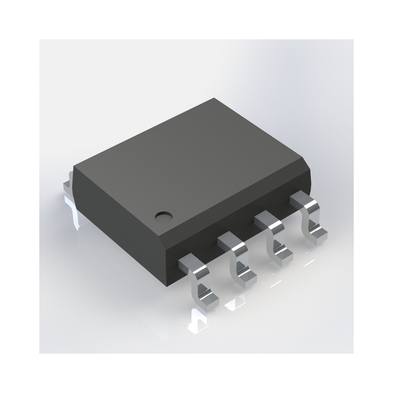
CDCLVC1104PWR
8-pin TSSOP package

CDCLVC1102PWR
Clock Fanout Buffer 2-OUT 1-IN 1:2 8-Pin TSSOP T/R

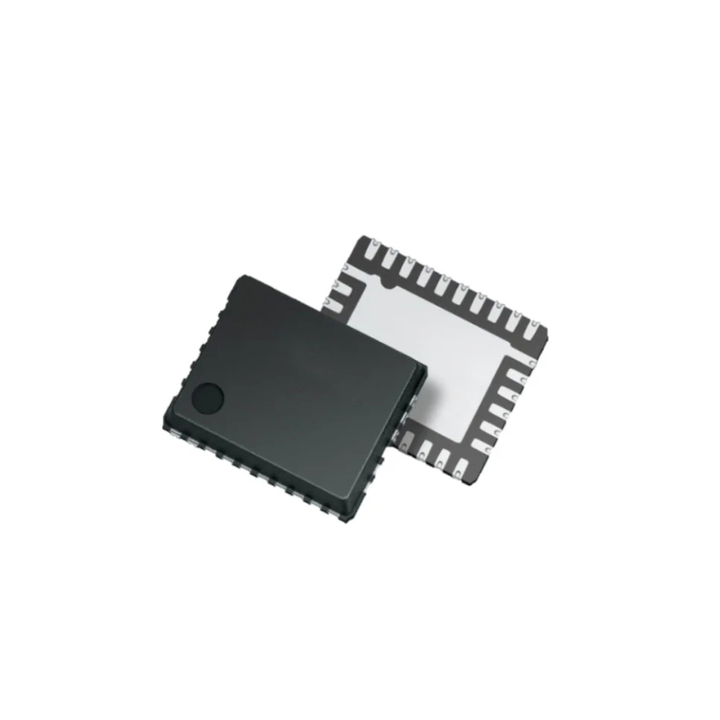
CDCI6214RGER
Clock Generators & Support Products PCIe Gen4 support ultra-low power clock generator with four programmable outputs & EEPROM 24-VQFN -40 to 85
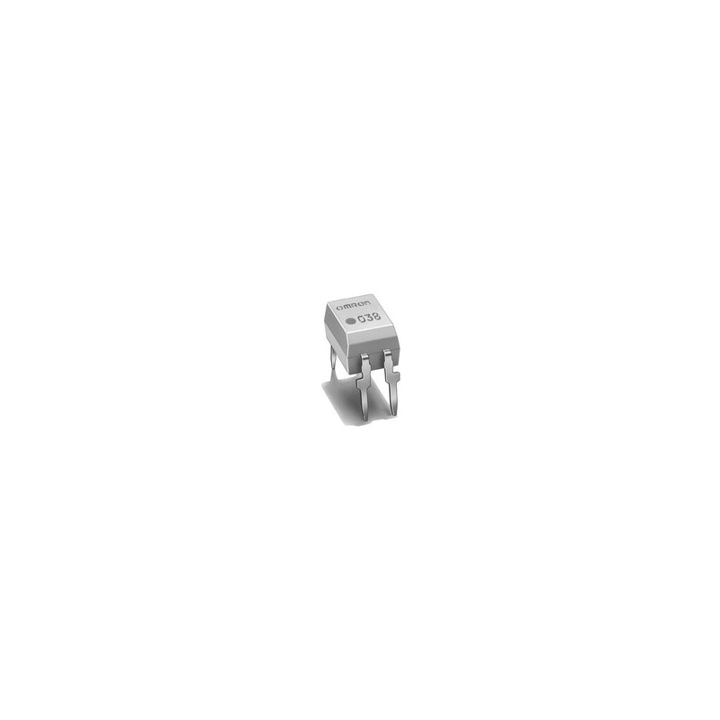
CD4046BEE4
CMOS Micropower phase locked loop
CDCVF2505D
Clock Drivers & Distribution 3.3V PLL Clock

CDCV304PWR
Versatile clock buffering solution for multiple devices
CDCE62002RHBT
The CDCE62002RHBT is a QFN-32-(5x5) clock generator, frequency synthesizer, and PLL that is ROHS compliant