
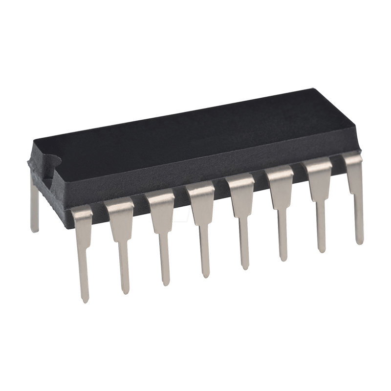
CD4081BE
Offering quad 2-input and gate functionality, CD4081BE is a member of the 4000, 14000, and 40000 series with a PDIP14 packaging
Inventory:6,341
- 90-day after-sales guarantee
- 365 Days Quality Guarantee
- Genuine Product Guarantee
- 7*24 hours service quarantee
-
Part Number : CD4081BE
-
Package/Case : PDIP (N)-14
-
Brands : Texas Instruments
-
Components Categories : Gates and Inverters
-
Datesheet : CD4081BE DataSheet (PDF)
The CD4081BE is a quad 2-input AND gate IC that offers versatile logic gate functionality in digital electronic circuits. With four independent AND gates, each with two inputs, this IC provides a compact and efficient solution for logical operations. (Note: The pin configuration below is a general representation. Refer to the specific datasheet for precise details.) Include a circuit diagram illustrating the connections and operation of the CD4081BE IC for a visual representation. Note: For detailed technical specifications, please refer to the CD4081BE datasheet. Functionality The CD4081BE is designed to perform logical AND operations on two input signals to produce the corresponding output. It is a versatile IC for implementing various logic functions in digital systems. Usage Guide Q: What is the maximum operating voltage for the CD4081BE? Q: Is the CD4081BE suitable for low-power applications? For alternatives with similar functionalities, consider these options to the CD4081BE:Overview of CD4081BE
Pinout
Circuit Diagram
Key Features
Application
Frequently Asked Questions
A: The CD4081BE can operate with a maximum supply voltage of 18V.
A: Yes, the CD4081BE features low power consumption, making it suitable for low-power and battery-operated devices.Equivalent
Specifications
The followings are basic parameters of the part selected concerning the characteristics of the part and categories it belongs to.
| Technology family | CD4000 | Supply voltage (min) (V) | 3 |
| Supply voltage (max) (V) | 18 | Number of channels | 4 |
| Inputs per channel | 2 | IOL (max) (mA) | 6.8 |
| IOH (max) (mA) | -6.8 | Input type | Standard CMOS |
| Output type | Push-Pull | Features | High speed (tpd 10- 50ns) |
| Data rate (max) (MBps) | 8 | Rating | Catalog |
| Operating temperature range (°C) | -55 to 125 |
Warranty & Returns
Warranty, Returns, and Additional Information
-
QA & Return Policy
Parts Quality Guarantee: 365 days
Returns for refund: within 90 days
Returns for Exchange: within 90 days
-
Shipping and Package
Shipping:For example, FedEx, SF, UPS, or DHL.UPS, or DHL.
Parts Packaging Guarantee: Featuring 100% ESD anti-static protection, our packaging incorporates high toughness and superior buffering capabilities.
-
Payment
For example, channels like VISA, MasterCard, UnionPay, Western Union, PayPal, and more.
If you have specific payment channel preferences or requirements, please get in touch with our sales team for assistance.
Similar Product

CD40106BCM
Inverter Schmitt Trigger 6-Element CMOS 14-Pin SOIC N Rail

CD40106BPW
Inverters Hex Schmitt Trigger

CD4514BCN
Multiplexers for binary signals
CD4503BCN
Buffers & Line Drivers Hex 3-STATE Buffer
CD4094BCN
Counter Shift Registers 8-Bit Shft Reg/Latch
CD4029BCN
Counter Shift Registers
CD4093BCMX
NAND Gate 4-Element 2-IN CMOS 14-Pin SOIC N T/R
CD4515BCN
The CD4515BCN offers engineers a reliable solution for managing data streams and making efficient use of limited resources in electronic systems