
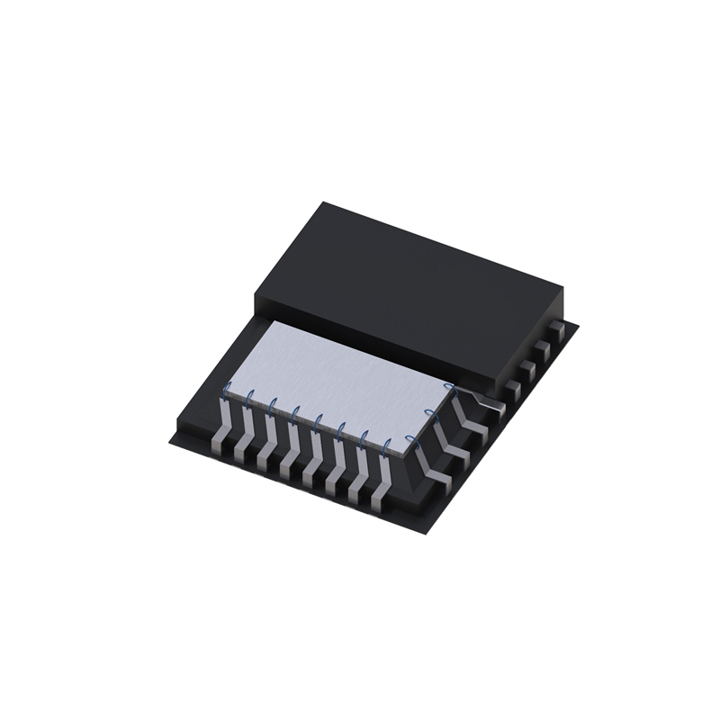
849N202CKI-999LF
FemtoClock NG Universal Frequency Translator
Inventory:3,941
- 90-day after-sales guarantee
- 365 Days Quality Guarantee
- Genuine Product Guarantee
- 7*24 hours service quarantee
-
Part Number : 849N202CKI-999LF
-
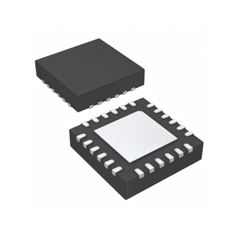
Package/Case : 40-VFQFN Exposed Pad
-
Brands : Renesas
-
Components Categories : Clock Generators, PLLs, Frequency Synthesizers
-
Datesheet : 849N202CKI-999LF DataSheet (PDF)
Overview of 849N202CKI-999LF
The 849N202I is a highly flexible FemtoClock® NG general purpose, low phase noise Universal Frequency Translator™ / Synthesizer with alarm and monitoring functions suitable for networking and communications applications. It is able to generate any output frequency in the 0.98MHz - 312.5MHz range and most output frequencies in the 312.5MHz - 1,300MHz range (see Table 3 for details). A wide range of input reference clocks and a range of low-cost fundamental mode crystal frequencies may be used as the source for the output frequency.
The 849N202I has three operating modes to support a very broad spectrum of applications.
To see other devices in this product family, visit the Universal Frequency Translators page.
Key Features
- 4TH generation FemtoClock® NG technology
- Universal Frequency Translator (UFT) / Frequency Synthesizer
- Two outputs, individually programmable as LVPECL or LVDS
Both outputs may be set to use 2.5V or 3.3V output levels
Programmable output frequency: 0.98MHz up to 1,300MHz - Zero ppm frequency translation
- Two differential inputs support the following input types:LVPECL, LVDS, LVHSTL, HCSL
- Input frequency range: 8kHz - 710MHz
- Crystal input frequency range: 16MHz - 40MHz
- Two factory-set register configurations for power-up default state
Power-up default configuration pin or register selectable
Configurations customized via One-Time Programmable ROM
Settings may be overwritten after power-up via I2C
I2C Serial interface for register programming - RMS phase jitter at 125MHz, using a 40MHz crystal(12kHz - 20MHz): 510fs (typical), Low Bandwidth Mode (FracN)
- RMS phase jitter at 400MHz, using a 40MHz crystal(12kHz - 40MHz): 321fs (typical), Synthesizer Mode (Integer FB)
- Output supply voltage modes:
VCC/VCCA/VCCO
3.3V/3.3V/3.3V
3.3V/3.3V/2.5V (LVPECL only)
2.5V/2.5V/2.5V - -40°C to 85°C ambient operating temperature
- Available in lead-free (RoHS 6) package
Specifications
The followings are basic parameters of the part selected concerning the characteristics of the part and categories it belongs to.
| Pkg. Type | VFQFPN | Lead Count (#) | 40 |
| Temp. Grade | I | Pb (Lead) Free | Yes |
| Carrier Type | Tray |
Warranty & Returns
Warranty, Returns, and Additional Information
-
QA & Return Policy
Parts Quality Guarantee: 365 days
Returns for refund: within 90 days
Returns for Exchange: within 90 days
-
Shipping and Package
Shipping:For example, FedEx, SF, UPS, or DHL.UPS, or DHL.
Parts Packaging Guarantee: Featuring 100% ESD anti-static protection, our packaging incorporates high toughness and superior buffering capabilities.
-
Payment
For example, channels like VISA, MasterCard, UnionPay, Western Union, PayPal, and more.
If you have specific payment channel preferences or requirements, please get in touch with our sales team for assistance.
Similar Product
ICS844021BGI-01LF
Clock Generator IC 170MHz 1 8-TSSOP (0.173", 4.40mm Width)

9DBL0841BKILF
Zero Delay Buffer Single 48-Pin VFQFPN Tray
M41ST84WMQ6E
STMicroelectronics M41ST84WMQ6E, Real Time Clock, 64B RAM Serial-I2C, 16-Pin SOIC
9FGL0841BKILF
Clock Generators & Support Products 8 O/P PCIE Gen 1-2-3 Clock Gen 100 Ohm
SY89847UMG
Clock Fanout Buffer 5-OUT 2-IN 1:5 32-Pin QFN EP Tube
CP82C84AZ
Clock Generators & Support Products W/ANNEAL PERIPH CLK GENERATOR 5V 25MHZ
ADCLK846BCPZ-REEL7
Clock Fanout Buffer 6-OUT 1-IN 1:6 24-Pin LFCSP EP T/R
ICS844071AGLF
Clock Generator IC 170MHz 1 8-TSSOP (0.173", 4.40mm Width)