
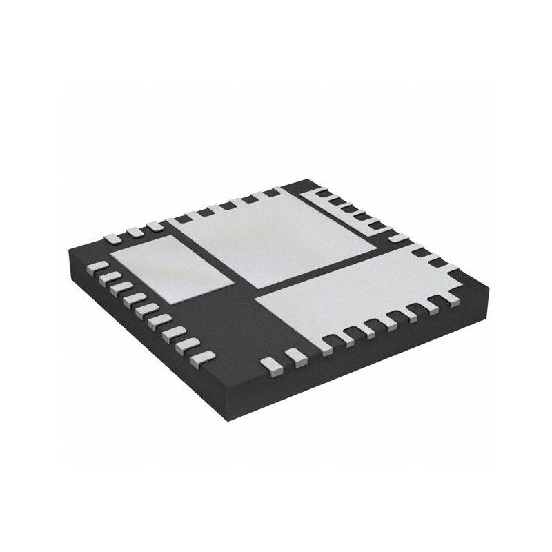
5T93GL10NLGI
2.5V LVDS,1:10 Glitchless Clock Buffer Terabuffer™ II
Inventory:4,657
- 90-day after-sales guarantee
- 365 Days Quality Guarantee
- Genuine Product Guarantee
- 7*24 hours service quarantee
-
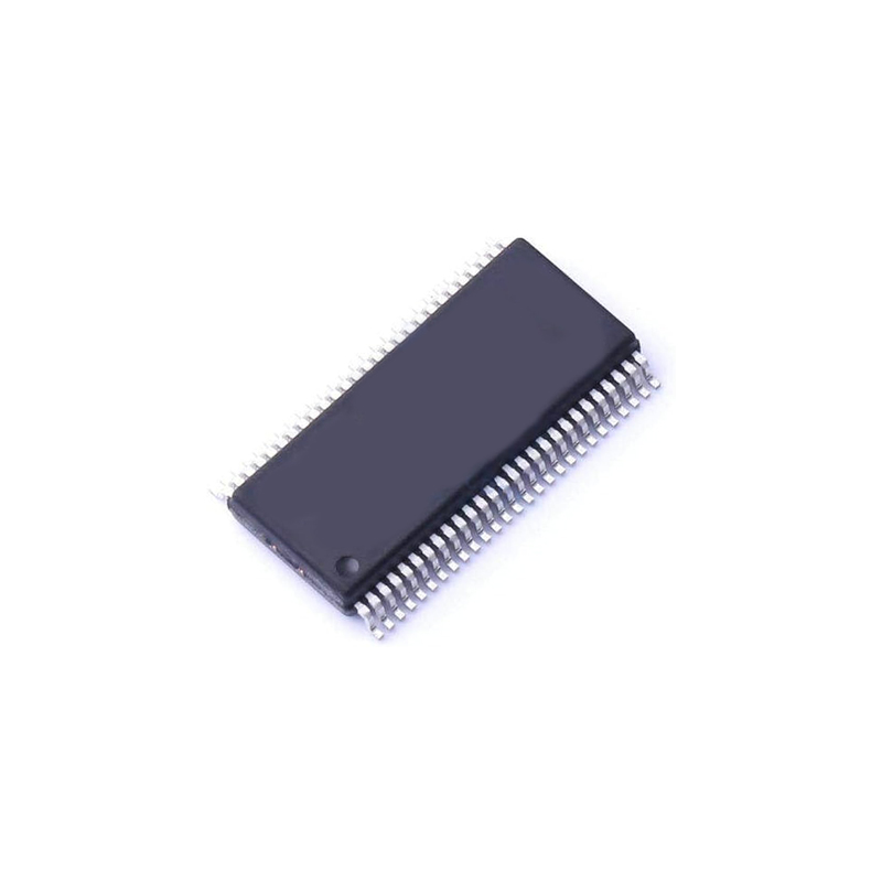
Part Number : 5T93GL10NLGI
-
Package/Case : 40-VFQFN Exposed Pad
-
Brands : Renesas
-
Components Categories : Clock Buffers, Drivers
-
Datesheet : 5T93GL10NLGI DataSheet (PDF)
Overview of 5T93GL10NLGI
The 5T93GL10 2.5V differential clock buffer is a user-selectable differential input to ten LVDS outputs. The fanout from a differential input to ten LVDS outputs reduces loading on the preceding driver and provides an efficient clock distribution network. The 5T93GL10 can act as a translator from a differential HSTL, eHSTL, LVEPECL (2.5V), LVPECL (3.3V), CML, or LVDS input to LVDS outputs. A single-ended 3.3V / 2.5V LVTTL input can also be used to translate to LVDS outputs. The redundant input capability allows for a glitchless change-over from a primary clock source to a secondary clock source. Selectable inputs are controlled by SEL. During the switchover, the output will disable low for up to three clock cycles of the previously-selected input clock. The outputs will remain low for up to three clock cycles of the newly-selected clock, after which the outputs will start from the newly-selected input. A FSEL pin has been implemented to control the switchover in cases where a clock source is absent or is driven to DC levels below the minimum specifications. The 5T93GL10 outputs can be asynchronously enabled/ disabled. When disabled, the outputs will drive to the value selected by the GL pin. Multiple power and grounds reduce noise.
Key Features
- Guaranteed low skew: <25ps (maximum)Very low duty cycle distortion: <100ps (maximum)High speed propagation delay: <2ns (maximum)Up to 650MHz operationGlitchless input clock switchingSelectable inputsHot insertable and over-voltage tolerant inputs3.3V/2.5V LVTTL, HSTL, eHSTL, LVEPECL (2.5V), LVPECL (3.3V), CML or LVDS input interfacesSelectable differential inputs to ten LVDS outputsPower-down modeAt power-up, FSEL should be LOW2.5V VDD-40°C to 85°C ambient operating temperatureAvailable in VFQFPN packageRecommends IDT5T9310 if glitchless input selection is not required
Specifications
The followings are basic parameters of the part selected concerning the characteristics of the part and categories it belongs to.
| Pkg. Type | VFQFPN | Lead Count (#) | 40 |
| Temp. Grade | I | Pb (Lead) Free | Yes |
| Carrier Type | Tray |
Warranty & Returns
Warranty, Returns, and Additional Information
-
QA & Return Policy
Parts Quality Guarantee: 365 days
Returns for refund: within 90 days
Returns for Exchange: within 90 days
-
Shipping and Package
Shipping:For example, FedEx, SF, UPS, or DHL.UPS, or DHL.
Parts Packaging Guarantee: Featuring 100% ESD anti-static protection, our packaging incorporates high toughness and superior buffering capabilities.
-
Payment
For example, channels like VISA, MasterCard, UnionPay, Western Union, PayPal, and more.
If you have specific payment channel preferences or requirements, please get in touch with our sales team for assistance.
Similar Product
5T9306NLGI
LVDS clock buffer with 2.5V power supply
TSA5055T
Phase Locked Loops - PLL

PCA8565TS
Real time clock/calendar
5T9310NLGI
Clock Buffer 2.5V LVDS 1:10 Clock Buffer
PCA21125T/Q900/1,1
NXP - PCA21125T/Q900/1,1 - REAL TIME CLOCK/CALENDAR, SPI, TSSOP-14
IDT5T9304EJGI
Clock Fanout Buffer (Distribution), Multiplexer IC 2:4 450 MHz 24-TSSOP (0.173", 4.40mm Width) Exposed Pad
IDT5T30553DCG8
Clock Fanout Buffer (Distribution) IC 1:4 200 MHz 8-SOIC (0.154", 3.90mm Width)
5T905PGGI8
2.5V Single Data Rate 1:5 Clock Buffer Terabuffer™