
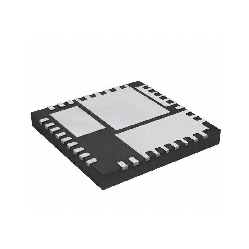
5T929-10NLGI
OC-48 Precision Clock Generator
Inventory:7,905
- 90-day after-sales guarantee
- 365 Days Quality Guarantee
- Genuine Product Guarantee
- 7*24 hours service quarantee
-
Part Number : 5T929-10NLGI
-
Package/Case : 28-VQFN Exposed Pad
-
Brands : Renesas
-
Components Categories : Application Specific Clock/Timing
-
Datesheet : 5T929-10NLGI DataSheet (PDF)
Overview of 5T929-10NLGI
The 5T929 generates a high precision FEC (Forward Error Correction) or non-FEC source clock for SONET/SDH systems as well as a source clock for Gigabit Ethernet systems. This device also has clock regeneration capability: it creates a "clean" version of the clock input by using the internal oscillator to square the input clock's rising and falling edges and remove jitter. In the event that the main clock input fails, the device automatically locks to a backup reference clock using a hitless switchover mechanism. This device detects loss of valid CLKIN and leaves the VCO of the PLL at the last valid frequency while an alternate input REFIN is selected. If CLKIN and REFIN are different frequencies, the multiplication factor will be adjusted to retain the same output frequency. The 5T929 can act as a translator from a differential LVPECL, LVDS, or single-ended LVTTL input to LVPECL or LVDS outputs. The 5T929-10 has LVDS outputs and the 5T929-30 has LVPECL outputs. The two modes of output frequency range are controlled by the SELmode. When SELmode is high or low, the QOUT is a multiplied version of the input clock while QREG is a regenerated version of the input clock.
Key Features
- Input frequency:
- For SONET non-FEC: 19.44MHz, 38.88MHz, 77.76MHz, 155.52MHz, 311.04MHz, or 622.08MHz
- For SONET FEC: 20.83MHz, 41.66MHz, 83.31MHz, 166.63MHz, 333.26MHz, or 666.52MHz
- For 10GE copper: 19.53MHz, 39.06MHz, 78.125MHz, 156.25MHz, 312.5MHz, or 625MHz
- For 10GE optical: 20.14MHz, 40.28MHz, 80.56MHz, 161.13MHz, 322.26MHz, or 644.53MHz
- Output frequency range selection
- 1x, 2x, 4x, 8x, 16x, and 32x outputs on QOUT
- Regenerated input clock on QREG
- Lock indicator
- Power-down mode
- LVPECL or LVDS outputs
- Two modes of output frequency range
- Mode 0: QOUT range 155.5 - 166.6MHz. QREG is a regenerated version of the input clock.
- Mode 1: QOUT range 622 - 666.5MHz. QREG is a regenerated version of the input clock frequency.
- Hitless switchover
- Differential LVPECL, LVDS, or single-ended LVTTL input interface
- 2.375 - 3.465V core and I/O
Specifications
The followings are basic parameters of the part selected concerning the characteristics of the part and categories it belongs to.
| Pkg. Type | VFQFPN | Lead Count (#) | 28 |
| Temp. Grade | I | Pb (Lead) Free | Yes |
| Carrier Type | Tray |
Warranty & Returns
Warranty, Returns, and Additional Information
-
QA & Return Policy
Parts Quality Guarantee: 365 days
Returns for refund: within 90 days
Returns for Exchange: within 90 days
-
Shipping and Package
Shipping:For example, FedEx, SF, UPS, or DHL.UPS, or DHL.
Parts Packaging Guarantee: Featuring 100% ESD anti-static protection, our packaging incorporates high toughness and superior buffering capabilities.
-
Payment
For example, channels like VISA, MasterCard, UnionPay, Western Union, PayPal, and more.
If you have specific payment channel preferences or requirements, please get in touch with our sales team for assistance.
Similar Product
5T9306NLGI
LVDS clock buffer with 2.5V power supply
TSA5055T
Phase Locked Loops - PLL

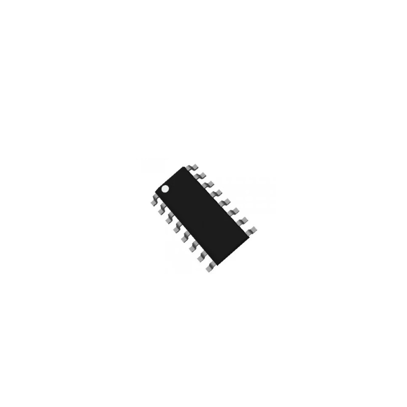
PCA8565TS
Real time clock/calendar
5T9310NLGI
Clock Buffer 2.5V LVDS 1:10 Clock Buffer
PCA21125T/Q900/1,1
NXP - PCA21125T/Q900/1,1 - REAL TIME CLOCK/CALENDAR, SPI, TSSOP-14
IDT5T9304EJGI
Clock Fanout Buffer (Distribution), Multiplexer IC 2:4 450 MHz 24-TSSOP (0.173", 4.40mm Width) Exposed Pad
IDT5T30553DCG8
Clock Fanout Buffer (Distribution) IC 1:4 200 MHz 8-SOIC (0.154", 3.90mm Width)
5T905PGGI8
2.5V Single Data Rate 1:5 Clock Buffer Terabuffer™