
5CGXFC7C6F23I7N
Programmable Logic Device
Inventory:9,425
- 90-day after-sales guarantee
- 365 Days Quality Guarantee
- Genuine Product Guarantee
- 7*24 hours service quarantee
-
Part Number : 5CGXFC7C6F23I7N
-
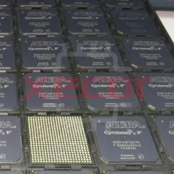
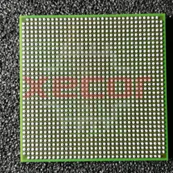
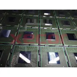
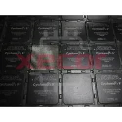
Package/Case : FBGA-484
-
Brands : Intel
-
Components Categories : FPGAs (Field Programmable Gate Array)
-
Datesheet : 5CGXFC7C6F23I7N DataSheet (PDF)
The 5CGXFC7C6F23I7N is a field-programmable gate array (FPGA) featuring a high-density design and advanced programmable logic capabilities. It is designed to provide flexible and customizable solutions for various digital design applications, including telecommunications, networking, and industrial automation. (Note: The pin configuration below is a general representation. Refer to the specific datasheet for precise details.) Include a circuit diagram illustrating the connections and operation of the 5CGXFC7C6F23I7N FPGA for a visual representation. Note: For detailed technical specifications, please refer to the 5CGXFC7C6F23I7N datasheet. Functionality The 5CGXFC7C6F23I7N FPGA is a versatile programmable device that enables users to implement custom digital designs with high flexibility and functionality. It serves as a key component in various digital applications requiring programmable logic solutions. Usage Guide Q: Can the 5CGXFC7C6F23I7N be reprogrammed multiple times? Q: What is the maximum operating frequency supported by the 5CGXFC7C6F23I7N? For similar functionalities, consider these alternatives to the 5CGXFC7C6F23I7N:Overview of 5CGXFC7C6F23I7N
Pinout
Circuit Diagram
Key Features
Application
Frequently Asked Questions
A: Yes, the FPGA can be reprogrammed multiple times to implement different designs or updates.
A: The FPGA supports high-speed operation with a maximum clock frequency specified in the datasheet.Equivalent
Specifications
The followings are basic parameters of the part selected concerning the characteristics of the part and categories it belongs to.
| Product Category | FPGA - Field Programmable Gate Array | RoHS | Details |
| Series | 5CGXFC7C | Number of Logic Elements | 150000 LE |
| Adaptive Logic Modules - ALMs | 56480 ALM | Embedded Memory | 7.696 Mbit |
| Number of I/Os | 240 I/O | Supply Voltage - Max | 1.1 V |
| Minimum Operating Temperature | - 40 C | Maximum Operating Temperature | + 100 C |
| Data Rate | 3.125 Gb/s | Number of Transceivers | 6 Transceiver |
| Mounting Style | SMD/SMT | Package / Case | FBGA-484 |
| Brand | Altera | Embedded Block RAM - EBR | 836 kbit |
| Maximum Operating Frequency | 925 MHz | Moisture Sensitive | Yes |
| Number of Logic Array Blocks - LABs | 5648 LAB | Operating Supply Voltage | 1.1 V |
| Product Type | FPGA - Field Programmable Gate Array | Factory Pack Quantity | 60 |
| Subcategory | Programmable Logic ICs | Total Memory | 7696 kbit |
| Tradename | Cyclone V | Part # Aliases | 969103 |
| Unit Weight | 0.742936 oz |
Warranty & Returns
Warranty, Returns, and Additional Information
-
QA & Return Policy
Parts Quality Guarantee: 365 days
Returns for refund: within 90 days
Returns for Exchange: within 90 days
-
Shipping and Package
Shipping:For example, FedEx, SF, UPS, or DHL.UPS, or DHL.
Parts Packaging Guarantee: Featuring 100% ESD anti-static protection, our packaging incorporates high toughness and superior buffering capabilities.
-
Payment
For example, channels like VISA, MasterCard, UnionPay, Western Union, PayPal, and more.
If you have specific payment channel preferences or requirements, please get in touch with our sales team for assistance.
Similar Product

5CEFA9F23I7N
PBGA484 Field Programmable Gate Array featuring 301000 Cells in CMOS
5CEFA2F23I7N
Reconfigurable hardware accelerator for various applications

5CEFA5F23I7N
1.1V Voltage Specification
EP2AGX260FF35C6N
FPGA Arria® II GX Family 244188 Cells 400MHz 40nm Technology 0.9V 1152-Pin FC-FBGA
EP2AGX45DF25C4N
FPGA Arria® II GX Family 42959 Cells 500MHz 40nm Technology 0.9V 572-Pin FC-FBGA Tray

EP4SGX230FF35C3N
FPGA - Field Programmable Gate Array FPGA - Stratix IV GX 9120 LABs 564 IOs
5CGTFD5C5F27C7N
FPGA Cyclone® V GT Family 77000 Cells 28nm Technology 1.1V 672-Pin FBGA

5CEFA9F31I7N
FPGA Cyclone® V E Family 301000 Cells 28nm Technology 1.1V 896-Pin FBGA