
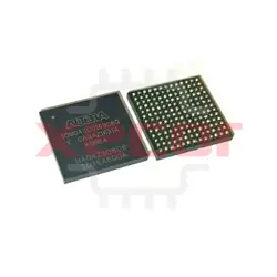
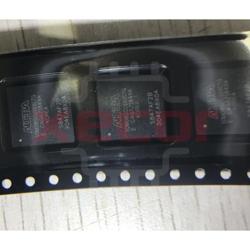
10M08SAU169C8G
FPGA - Field Programmable Gate Array
Inventory:5,990
- 90-day after-sales guarantee
- 365 Days Quality Guarantee
- Genuine Product Guarantee
- 7*24 hours service quarantee
-
Part Number : 10M08SAU169C8G
-
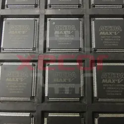
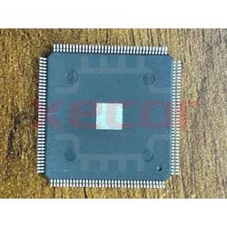
Package/Case : BGA-169
-
Brands : Intel
-
Components Categories : FPGAs (Field Programmable Gate Array)
-
Datesheet : 10M08SAU169C8G DataSheet (PDF)
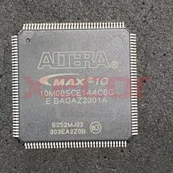
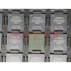
The 10M08SAU169C8G is a low-cost, low-power field-programmable gate array (FPGA) that offers a versatile and reconfigurable solution for various digital design applications. This FPGA features 8,000 logic elements and is suitable for implementing small to medium-scale digital circuits. (Note: The pin configuration below is a general representation. Refer to the specific datasheet for precise details.) Include a circuit diagram illustrating the connections and operation of the 10M08SAU169C8G FPGA for a visual representation. Note: For detailed technical specifications, please refer to the 10M08SAU169C8G FPGA datasheet. Functionality The 10M08SAU169C8G FPGA provides a customizable logic platform for designing digital systems with specific functionality requirements. It offers flexibility and performance in a compact package. Usage Guide Q: Can the 10M08SAU169C8G be reprogrammed multiple times? Q: What tools are recommended for programming the 10M08SAU169C8G FPGA? For similar functionalities, consider these alternatives to the 10M08SAU169C8G FPGA:Overview of 10M08SAU169C8G
Pinout
Circuit DiagramKey Features
Application
Frequently Asked Questions
A: Yes, the 10M08SAU169C8G is a reprogrammable FPGA that can be reconfigured multiple times as needed for different applications.
A: To program the 10M08SAU169C8G FPGA, you can use FPGA development software such as Quartus Prime from Intel (formerly Altera) or similar tools provided by the FPGA manufacturer.Equivalent
Specifications
The followings are basic parameters of the part selected concerning the characteristics of the part and categories it belongs to.
| Product Category | FPGA - Field Programmable Gate Array | RoHS | Details |
| Series | MAX 10 10M08 | Number of Logic Elements | 8000 LE |
| Embedded Memory | 378 kbit | Number of I/Os | 130 I/O |
| Supply Voltage - Min | 2.85 V | Supply Voltage - Max | 3.465 V |
| Minimum Operating Temperature | 0 C | Maximum Operating Temperature | + 85 C |
| Mounting Style | SMD/SMT | Package / Case | UBGA-169 |
| Brand | Altera | Length | 11 mm |
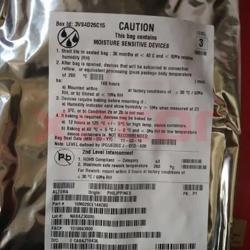
| Maximum Operating Frequency | 450 MHz | Moisture Sensitive | Yes |
| Number of Logic Array Blocks - LABs | 500 LAB | Operating Supply Voltage | 3 V, 3.3 V |
| Product Type | FPGA - Field Programmable Gate Array | Factory Pack Quantity | 176 |
| Subcategory | Programmable Logic ICs | Tradename | MAX |
| Width | 11 mm | Part # Aliases | 968101 |
| Unit Weight | 0.423288 oz |
Warranty & Returns
Warranty, Returns, and Additional Information
-
QA & Return Policy
Parts Quality Guarantee: 365 days
Returns for refund: within 90 days
Returns for Exchange: within 90 days
-
Shipping and Package
Shipping:For example, FedEx, SF, UPS, or DHL.UPS, or DHL.
Parts Packaging Guarantee: Featuring 100% ESD anti-static protection, our packaging incorporates high toughness and superior buffering capabilities.
-
Payment
For example, channels like VISA, MasterCard, UnionPay, Western Union, PayPal, and more.
If you have specific payment channel preferences or requirements, please get in touch with our sales team for assistance.
Similar Product
5M570ZT100C5N
CPLD - Complex Programmable Logic Devices CPLD - MAX V 440 Macro 74 IOs
10M02SCE144I7G
FPGA - Field Programmable Gate Array non-volatile FPGA, 101 I/O, 144EQFP
10M02SCE144C8G
FPGA MAX 10 Family 2000 Cells 55nm Technology 1.2V 144-Pin EQFP EP Tray
10M04SCU169C8G
FPGA MAX 10 Family 4000 Cells 55nm Technology 1.2V 169-Pin UBGA Tray
10M08SCU169I7G
FPGA - Field Programmable Gate Array non-volatile FPGA, 130 I/O, 169UBGA
10M08SCE144C8G
FPGA - Field Programmable Gate Array non-volatile FPGA, 101 I/O, 144EQFP
10M08SAU169I7G
FPGA - Field Programmable Gate Array
10M16SCU324I7G
FPGA MAX 10 Family 16000 Cells 55nm Technology 1.2V 324-Pin UBGA