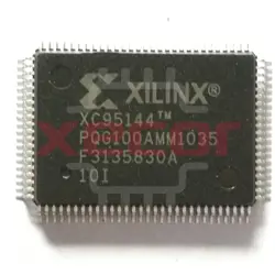
XC95144-10PQG100I
The device operates at a clock frequency of 66.7MHz and is built using 0.5um technology for optimal performance
Inventory:5,554
- 90-day after-sales guarantee
- 365 Days Quality Guarantee
- Genuine Product Guarantee
- 7*24 hours service quarantee
-
Part Number : XC95144-10PQG100I
-
Package/Case : QFP100
-
Brand : Xilinx
-
Components Classification : Controllers
-
Datesheet : XC95144-10PQG100I DataSheet (PDF)
The XC95144-10PQG100I is a field-programmable gate array (FPGA) IC featuring 114,480 logic cells, 4,608 configuration flip-flops, and a maximum of 10ns pin-to-pin delay. It offers versatile programmable logic capabilities for digital design applications, making it suitable for prototyping, testing, and implementation of custom logic functions. (Note: The pinout information provided below is a general representation. Refer to the specific datasheet for precise details.) Include a circuit diagram illustrating the connections and operation of the XC95144-10PQG100I FPGA for a better visual understanding of its functionality. Note: For detailed technical specifications, please refer to the XC95144-10PQG100I datasheet. Functionality The XC95144-10PQG100I FPGA provides a flexible and programmable logic platform for implementing custom digital circuits and functions. It offers designers a versatile tool for developing complex digital systems. Usage Guide Q: Can the XC95144-10PQG100I be reprogrammed multiple times? Q: What is the maximum logic cell count for the XC95144-10PQG100I? For alternative FPGA options with similar capabilities, consider these products:Overview of XC95144-10PQG100I
Pinout
Circuit Diagram
Key Features
Application
Frequently Asked Questions
A: Yes, the XC95144-10PQG100I FPGA is reprogrammable and can be configured multiple times for iterative design processes.
A: The XC95144-10PQG100I FPGA features 114,480 logic cells for extensive digital design capabilities.Equivalent
Specifications
The followings are basic parameters of the part selected concerning the characteristics of the part and categories it belongs to.
| Product Category | Xilinx | Brand | Xilinx |
Warranty & Returns
Warranty, Returns, and Additional Information
-
QA & Return Policy
Parts Quality Guarantee: 365 days
Returns for refund: within 90 days
Returns for Exchange: within 90 days
-
Shipping and Package
Shipping:For example, FedEx, JP, UPS, DHL,SAGAWA, or YTC.
Parts Packaging Guarantee: Featuring 100% ESD anti-static protection, our packaging incorporates high toughness and superior buffering capabilities.
-
Payment
For example, channels like VISA,MasterCard,Western Union,PayPal,MoneyGram,Rakuten Pay and more.
If you have specific payment channel preferences or requirements, please get in touch with our sales team for assistance.

XCF16PFSG48C
Field-Programmable Gate Array Memory

XCF02SVO20C
2Mb configuration memory flash

XCCACE-TQG144I
System Ace CF Controller

XC17S20PD8C
volatile memory chip

XC18V01PC20C
XC18V01PC20C PLCC-20 Memory - Configuration Proms for FPGAs ROHS

XC18V01PCG20C
Configuration Proms

XC17S40PD8C
Integrated Circuit for Programmable Logic Configuration

XC18V02VQG44C
Description Product Development Demo

XCF08PFSG48C
XCF08P - PROMs for In-System Programming of Platform Configurations

CY7C131-55JXC
CY7C131-55JXC, SRAM Memory 8kbit, 1K words x 8 bit, 5V, 52-Pin, PLCC

