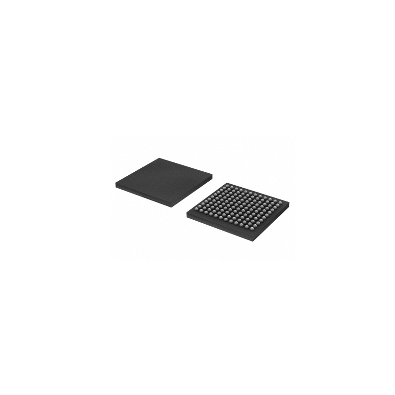
XC2VP30-5FG676I
XC2VP30-5FG676I Field Programmable Gate Array
Inventory:6,422
- 90-day after-sales guarantee
- 365 Days Quality Guarantee
- Genuine Product Guarantee
- 7*24 hours service quarantee
-
Part Number : XC2VP30-5FG676I
-
Package/Case : BGA-676
-
Brands : AMD
-
Components Categories : FPGAs
-
Datesheet : XC2VP30-5FG676I DataSheet (PDF)
The XC2VP30-5FG676I is a Virtex-II Pro FPGA (Field-Programmable Gate Array) from Xilinx, offering high-performance programmable logic capabilities for various applications. It features 30,000 logic cells, 320 I/O pins, and advanced features for complex digital designs. (Note: The pin configuration below is a general representation. Refer to the specific datasheet for precise details.) Include a circuit diagram illustrating the connections and operation of the XC2VP30-5FG676I FPGA for visual reference. Note: For detailed technical specifications, please refer to the XC2VP30-5FG676I datasheet. Functionality The XC2VP30-5FG676I FPGA offers reconfigurable logic resources that can be programmed to perform a wide range of functions, making it versatile for different applications requiring programmable logic. Usage Guide Q: Can the XC2VP30-5FG676I be cascaded with other FPGAs? Q: What tools are recommended for programming the XC2VP30-5FG676I? For similar FPGA solutions, consider these alternatives to the XC2VP30-5FG676I:Overview of XC2VP30-5FG676I
Pinout
Circuit Diagram
Key Features
Application
Frequently Asked Questions
A: Yes, the XC2VP30-5FG676I can be cascaded or used in conjunction with other FPGAs for enhanced processing capabilities.
A: Xilinx provides software tools like Vivado for programming, configuring, and debugging the XC2VP30-5FG676I FPGA.Equivalent
Specifications
The followings are basic parameters of the part selected concerning the characteristics of the part and categories it belongs to.
| Series | Virtex®-II Pro | Package | Tray |
| Product Status | Obsolete | Programmable | Not Verified |
| Number of LABs/CLBs | 3424 | Number of Logic Elements/Cells | 30816 |
| Total RAM Bits | 2506752 | Number of I/O | 416 |
| Voltage - Supply | 1.425V ~ 1.575V | Mounting Type | Surface Mount |
| Operating Temperature | -40°C ~ 100°C (TJ) | Package / Case | 676-BGA |
| Supplier Device Package | 676-FBGA (27x27) | Base Product Number | XC2VP30 |
Warranty & Returns
Warranty, Returns, and Additional Information
-
QA & Return Policy
Parts Quality Guarantee: 365 days
Returns for refund: within 90 days
Returns for Exchange: within 90 days
-
Shipping and Package
Shipping:For example, FedEx, JP, UPS, DHL,SAGAWA, or YTC.
Parts Packaging Guarantee: Featuring 100% ESD anti-static protection, our packaging incorporates high toughness and superior buffering capabilities.
-
Payment
For example, channels like VISA,MasterCard,Western Union,PayPal,MoneyGram,Rakuten Pay and more.
If you have specific payment channel preferences or requirements, please get in touch with our sales team for assistance.

XC3042A-7PC84C
This product is a Programmable Logic IC that utilizes CMOS technology and features SMT for easy installation

XC3S100E-4VQG100I
English expressions: Sort, Return, Sort, Gates

XC3S250E-4VQG100I
XC3S250E-4VQG100I is a versatile FPGA for development

XC3S50-4VQG100C
90nm Technology

XC56309AG100A
Digital Signal Processor, 24-Ext Bit, 100MHz, CMOS, PQFP144

XC5VFX130T-2FFG1738I
XC5VFX130T-2FFG1738I FPGA featuring 10240 Configurable Logic Blocks and 13172 logic cells

XC5VFX30T-1FFG665I
Versatile integration of customizable logic functions

XC6SLX75-2FGG484I
XILINX - XC6SLX75-2FGG484I - FPGA, SPARTAN-6 LX, 74K, 484FGGBGA

XC6VLX130T-2FFG784I
Get ready to elevate your development process with the XC6VLX130T-2FFG784I and unlock endless possibilities

XC7A75T-2FGG676I
With ROHS compliance and a FBGA-676 package, this programmable logic device offers flexibility for CPLDs/FPGAs

