
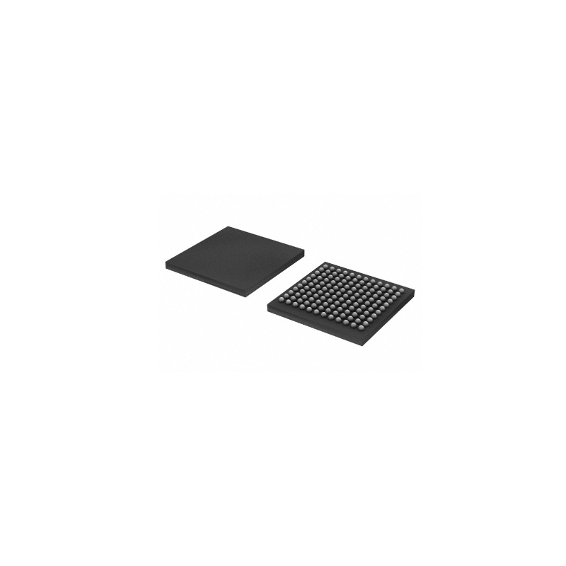
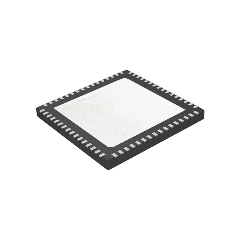
TS3DDR4000ZBAR
Multiplexer Switch ICs 3.3-V, 2:1 (SPDT), 12-channel DDR2, DDR3 & DDR4 switch 48-NFBGA -40 to 85
Inventory:2,315
- 90-day after-sales guarantee
- 365 Days Quality Guarantee
- Genuine Product Guarantee
- 7*24 hours service quarantee
-
Part Number : TS3DDR4000ZBAR
-
Package/Case : NFBGA (ZBA)-48
-
Brand : TI
-
Components Classification : Analog Switches , Special Purpose
-
Datesheet : TS3DDR4000ZBAR DataSheet (PDF)
The TS3DDR4000ZBAR is a high-speed ddr/lpddr3/4 termination regulator designed to provide accurate voltage regulation for memory interfaces.This regulator offers a compact and efficient solution for ensuring stable power supply to DDR/LPDDR memory modules. (Note:The pin configuration below is a general representation.Refer to the specific datasheet for precise details.) Include a circuit diagram illustrating the connections and operation of the TS3DDR4000ZBAR IC for a visual representation. Note:For detailed technical specifications,please refer to the TS3DDR4000ZBAR datasheet. Functionality The TS3DDR4000ZBAR is specifically designed to regulate termination voltages in DDR and LPDDR memory interfaces,ensuring reliable and high-performance operation of memory modules in electronic systems. Usage Guide Q:What is the operating voltage range of the TS3DDR4000ZBAR? Q:Does the TS3DDR4000ZBAR offer thermal protection? For similar functionalities,consider these alternatives to the TS3DDR4000ZBAR:Overview of TS3DDR4000ZBAR
Pinout
Circuit DiagramKey Features
Application
Frequently Asked Questions
A:The TS3DDR4000ZBAR operates within a specified voltage range, typically from 1.2V to 3.6V, for memory interface applications.
A:Yes, the TS3DDR4000ZBAR includes thermal protection features to prevent overheating and ensure safe operation of the memory interface.Equivalent
Specifications
The followings are basic parameters of the part selected concerning the characteristics of the part and categories it belongs to.
| Protocols | DDR2, DDR3, DDR4, MIPI | Configuration | 2:1 SPDT |
| Number of channels | 12 | Supply voltage (max) (V) | 3.6 |
| Supply voltage (min) (V) | 2.375 | Ron (typ) (mΩ) | 8300 |
| Input/output voltage (min) (V) | 0 | Input/output voltage (max) (V) | 3.3 |
| Supply current (typ) (µA) | 40 | ESD HBM (typ) (kV) | 3 |
| Operating temperature range (°C) | -40 to 85 | Crosstalk (dB) | -68 |
| COFF (typ) (pF) | 1 | CON (typ) (pF) | 0.5 |
| Off isolation (typ) (dB) | -34 | OFF-state leakage current (max) (µA) | 5 |
| Ron (max) (mΩ) | 11200 | Ron channel match (max) (Ω) | 1 |
| RON flatness (typ) (Ω) | 0.6 | Turnoff time (disable) (max) (ns) | 65 |
| Turnon time (enable) (max) (ns) | 65 | VIH (min) (V) | 1.4 |
| VIL (max) (V) | 0.5 |
Warranty & Returns
Warranty, Returns, and Additional Information
-
QA & Return Policy
Parts Quality Guarantee: 365 days
Returns for refund: within 90 days
Returns for Exchange: within 90 days
-
Shipping and Package
Shipping:For example, FedEx, JP, UPS, DHL,SAGAWA, or YTC.
Parts Packaging Guarantee: Featuring 100% ESD anti-static protection, our packaging incorporates high toughness and superior buffering capabilities.
-
Payment
For example, channels like VISA,MasterCard,Western Union,PayPal,MoneyGram,Rakuten Pay and more.
If you have specific payment channel preferences or requirements, please get in touch with our sales team for assistance.

TS3USB221DRCR
USB Switch ICs HS USB 2.0 (480Mbps) 1:2 Multiplexer/De

TS3USB31RSER
CMOS 8-pin IC with rail-to-rail input/output and 10MHz operational amplifier capability

TS5A3357DCUR
High-speed analog switch for precise signal routing and multiplexing application

TS5A3157DCKR
Analog Switch Single SPDT 6-Pin SC-70 T/R

TS3A5018RSVR
The TS3A5018RSVR features a compact 16-UQFN package, making it suitable for space-constrained designs

TS5A3167DCKR
Analog Switch ICs 1-Ohm SPST 5-V/3.3-V Sng-Ch Analog Switc

TS5A23159DGSR
2-channel SPDT analog switch with 1-ohm on-state resistance, suitable for -40 to 85 degree Celsius environments

TS3A27518ERTWR
High-performance signal routing solution

TS3A44159RGTR
High-performance signal switch with four channels and 2:1 multiplexer configuration

TS3A44159PWR
Versatile 4-channel on-state switch
ST232ECN
High-speed serial communication solution for industrial applications
ISD15108FYI
This product, ISD15108FYI, allows for voice recording and playback for up to 480 seconds, with an impedance of 80kOhm and a 3.3V power requirement
SP334CT-L
3/5 SOIC-28-300mil IC designed for 235Kbps RS232 communication
AQR107-B0-EG-Y
Marvell Semiconductor Europa 7x11 10G single port

ADG1408YRUZ-REEL7
This IC is designed to efficiently switch between multiple input signals with minimal added resistance
PCM3168APAPR
General Purpose Audio Codec 6ADC / 8DAC Ch 64-Pin HTQFP EP T/R
PCA82C250T/YM,118
Product on tape
SN65175D
With its quadruple differential line receiver function
MAX3221EIPW
With its 16-pin TSSOP format, this single transmitter/receiver chip offers a versatile option for RS-232 applications."
HV2901K6-G
Analog Switch ICs 32CH HV 200V ANALOG SWITCH