
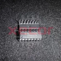
MC14042BCP
Latches 3-18V Quad
| Quantity | Unit Price(USD) | Ext. Price |
|---|---|---|
| 1 | $0.323 | $0.32 |
| 200 | $0.125 | $25.00 |
| 500 | $0.120 | $60.00 |
| 1000 | $0.118 | $118.00 |
Inventory:7,366
- 90-day after-sales guarantee
- 365 Days Quality Guarantee
- Genuine Product Guarantee
- 7*24 hours service quarantee
-
Part Number : MC14042BCP
-
Package/Case : PDIP-16
-
Brand : Onsemi
-
Components Classification : Latches
-
Datesheet : MC14042BCP DataSheet (PDF)
The MC14042BCP is a versatile CMOS dual 4-stage shift register IC designed for digital logic applications. This IC features two independent 4-bit shift registers that can be cascaded for extended shift register operation. (Note: The pin configuration below is a general representation. Refer to the specific datasheet for precise details.) Include a circuit diagram illustrating the connections and operation of the MC14042BCP IC for a visual representation. Note: For detailed technical specifications, please refer to the MC14042BCP datasheet. Functionality The MC14042BCP is a dual 4-stage shift register IC that enables sequential data storage and manipulation in digital systems. It offers high flexibility and reliability for various sequential logic applications. Usage Guide Q: Can the MC14042BCP operate at higher voltages? Q: Is the MC14042BCP compatible with TTL logic levels? For similar functionalities, consider these alternatives to the MC14042BCP:Overview of MC14042BCP
Pinout
Circuit Diagram
Key Features
Application
Frequently Asked Questions
A: The MC14042BCP is designed to operate within a voltage range of +3V to +18V. Operating beyond this range may result in IC damage.
A: Yes, the MC14042BCP can interface with TTL logic levels due to its CMOS technology characteristics.Equivalent
Specifications
The followings are basic parameters of the part selected concerning the characteristics of the part and categories it belongs to.
| Product Category | Latches | RoHS | N |
| Number of Circuits | 4 Circuit | Logic Type | Transparent Latch |
| Logic Family | MC14 | Polarity | Inverting, Non-Inverting |
| Quiescent Current | 4 uA | Number of Output Lines | 4 Line |
| High Level Output Current | - 4.2 mA | Low Level Output Current | 32 mA |
| Propagation Delay Time | 440 ns at 5 V, 180 ns at 10 V, 120 ns at 15 V | Supply Voltage - Max | 18 V |
| Supply Voltage - Min | 3 V | Minimum Operating Temperature | - 55 C |
| Maximum Operating Temperature | + 125 C | Package / Case | PDIP-16 |
| Brand | onsemi | Function | Transparent |
| Height | 3.43 mm | Length | 19.55 mm |
| Mounting Style | Through Hole | Number of Channels | 4 Channels |
| Number of Input Lines | 4 Line | Operating Supply Voltage | 3 V to 18 V |
| Product Type | Latches | Reset Type | No Reset |
| Factory Pack Quantity | 25 | Subcategory | Logic ICs |
| Supply Current - Max | 6 nA | Type | D-Type |
| Width | 6.85 mm | Unit Weight | 0.057419 oz |
Warranty & Returns
Warranty, Returns, and Additional Information
-
QA & Return Policy
Parts Quality Guarantee: 365 days
Returns for refund: within 90 days
Returns for Exchange: within 90 days
-
Shipping and Package
Shipping:For example, FedEx, JP, UPS, DHL,SAGAWA, or YTC.
Parts Packaging Guarantee: Featuring 100% ESD anti-static protection, our packaging incorporates high toughness and superior buffering capabilities.
-
Payment
For example, channels like VISA,MasterCard,Western Union,PayPal,MoneyGram,Rakuten Pay and more.
If you have specific payment channel preferences or requirements, please get in touch with our sales team for assistance.

MC14528BCP
Multivibrator with Monostable Type

MC14013BDR2G
MC14013BDR2G Flip Flops: Dual D-Type Functionality for 3-18V Voltage Range

MC14094BDR2G
Versatile 16-Pin SOIC Package with Tape/Reel Packaging
MC14027BCPG
Operating voltage range of 3-18V for the dual JK-type CMOS flip flops

MC74VHC1G08DFT2G
AND Gate 1-Element 2-IN CMOS 5-Pin SC-88A T/R
MC10ELT24DG
The MC10ELT24DG operates at a frequency of 400 MHz
MC100ELT21DG
Unidirectional communication conversion
MC14504BCP
Voltage Translator
MC14553BCP
Counter Shift Registers 3-18V 3-Digit BCD
MC14557BCP
3-18V Counter Shift Registers with 1-64 Bit functionality