M2S090TS-1FG676I
65nm Technology FPGA SmartFusion2 Family with 1.2V voltage
Inventory:7,498
- 90-day after-sales guarantee
- 365 Days Quality Guarantee
- Genuine Product Guarantee
- 7*24 hours service quarantee
-
Part Number : M2S090TS-1FG676I
-
Package/Case : BGA-676
-
Brands : Microchip Technology
-
Components Categories : System On Chip
-
Datesheet : M2S090TS-1FG676I DataSheet (PDF)
The M2S090TS-1FG676I is a low-power, high-performance FPGA (Field-Programmable Gate Array) designed to provide reconfigurable logic for various digital design applications. With a range of features and capabilities, this FPGA offers flexibility and scalability for complex system designs. (Note: The pin configuration below is a general representation. Refer to the specific datasheet for precise details.) Include a circuit diagram illustrating the connections and operation of the M2S090TS-1FG676I for a visual representation. Note: For detailed technical specifications, please refer to the M2S090TS-1FG676I datasheet. Functionality The M2S090TS-1FG676I FPGA provides reconfigurable logic elements, allowing users to implement custom logic functions tailored to their specific application requirements. It offers a versatile platform for digital design and implementation. Usage Guide Q: Can the M2S090TS-1FG676I be reprogrammed multiple times? Q: What is the typical power consumption of the M2S090TS-1FG676I in active mode? For similar functionalities, consider these alternatives to the M2S090TS-1FG676I:Overview of M2S090TS-1FG676I
Pinout
Circuit Diagram
Key Features
Application
Frequently Asked Questions
A: Yes, the M2S090TS-1FG676I FPGA supports multiple reprogramming cycles, allowing for flexibility in design iterations and updates.
A: The typical power consumption in active mode is specified in the datasheet and should be considered based on the application requirements.Equivalent
Specifications
The followings are basic parameters of the part selected concerning the characteristics of the part and categories it belongs to.
| Product Category | SoC FPGA | RoHS | N |
| Mounting Style | SMD/SMT | Package / Case | BGA-676 |
| Core | ARM Cortex M3 | Number of Cores | 1 Core |
| Maximum Clock Frequency | 166 MHz | Program Memory Size | 512 kB |
| Data RAM Size | 64 kB | Number of Logic Elements | 86316 LE |
| Brand | Microchip Technology | Moisture Sensitive | Yes |
| Number of Logic Array Blocks - LABs | 7193 LAB | Product Type | SoC FPGA |
| Series | SmartFusion2 | Factory Pack Quantity | 40 |
| Subcategory | SOC - Systems on a Chip | Unit Weight | 1.071118 oz |
Warranty & Returns
Warranty, Returns, and Additional Information
-
QA & Return Policy
Parts Quality Guarantee: 365 days
Returns for refund: within 90 days
Returns for Exchange: within 90 days
-
Shipping and Package
Shipping:For example, FedEx, JP, UPS, DHL,SAGAWA, or YTC.
Parts Packaging Guarantee: Featuring 100% ESD anti-static protection, our packaging incorporates high toughness and superior buffering capabilities.
-
Payment
For example, channels like VISA,MasterCard,Western Union,PayPal,MoneyGram,Rakuten Pay and more.
If you have specific payment channel preferences or requirements, please get in touch with our sales team for assistance.

MCF5329CVM240
High-performance computing solution
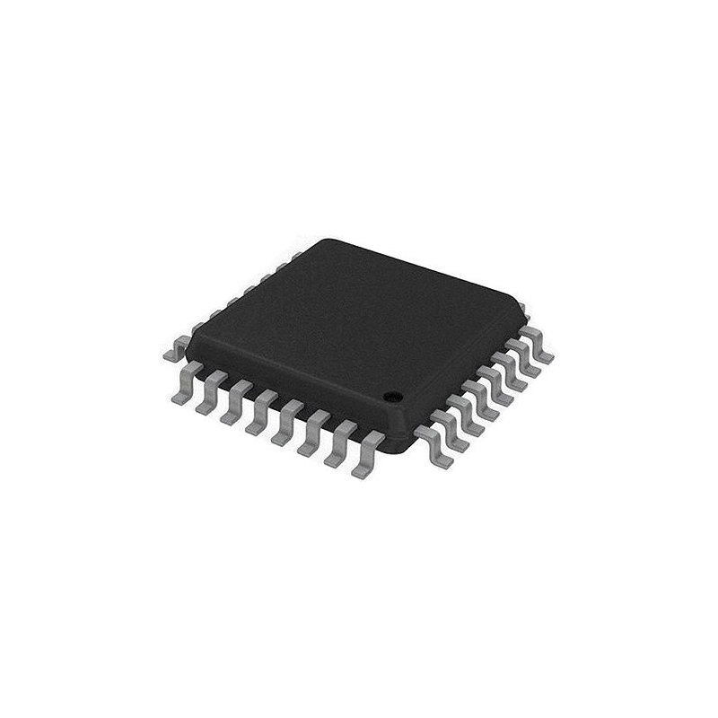
MCF51MM256CLL
MCU 32-bit ColdFire RISC 256KB Flash 2.5V/3.3V 100-Pin LQFP Tray
MC9328MX1VM20
SOC i.MX1 ARM9TDMI
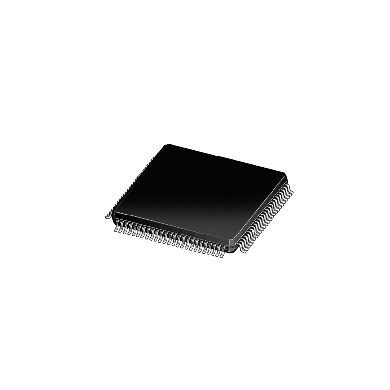
R7FA4M2AD3CFP#AA0
100MHz, LQFP-100 Package

MCF51EM256CLL
32-bit MCU with extensive capabilities
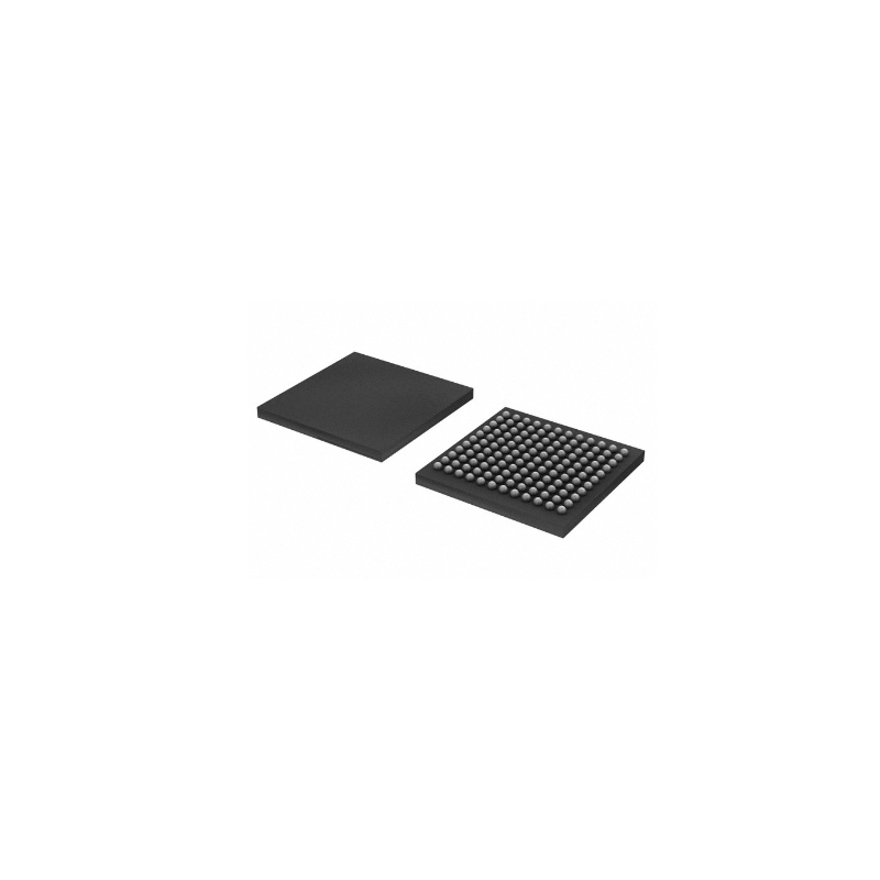
MCF5373LCVM240
MPU MCF53xx RISC 32-Bit CMOS 240MHz 196-Pin MA-BGA Tray
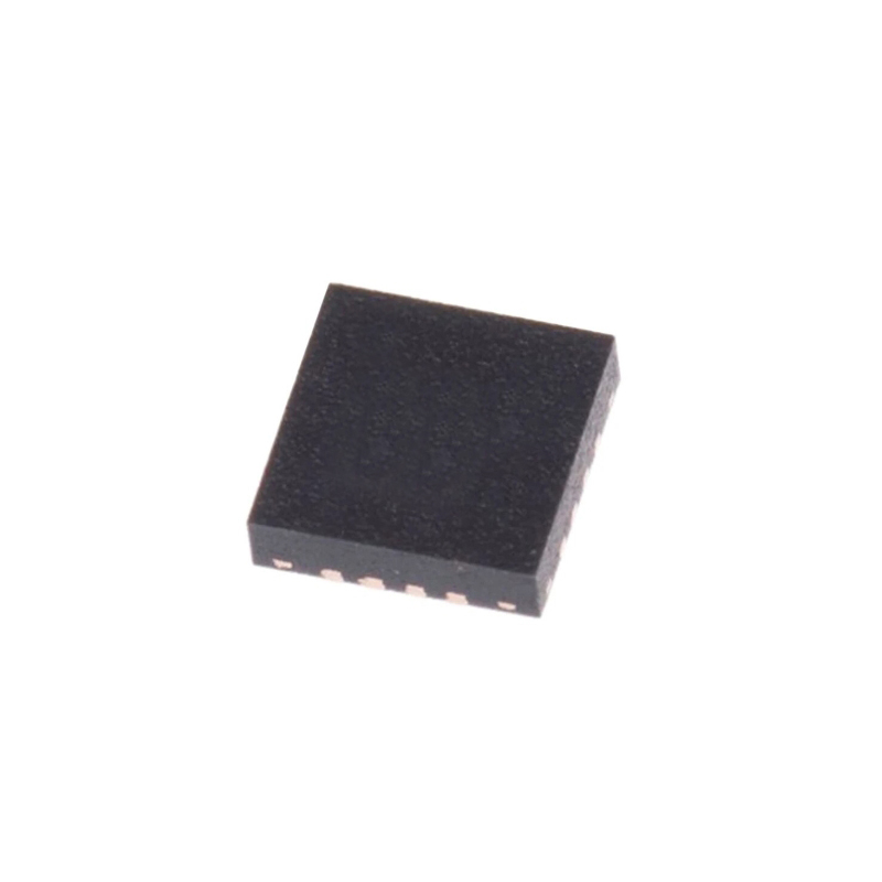
LPC824M201JHI33Y
Low-power high-performance microcontroller with 32KB Flash memory
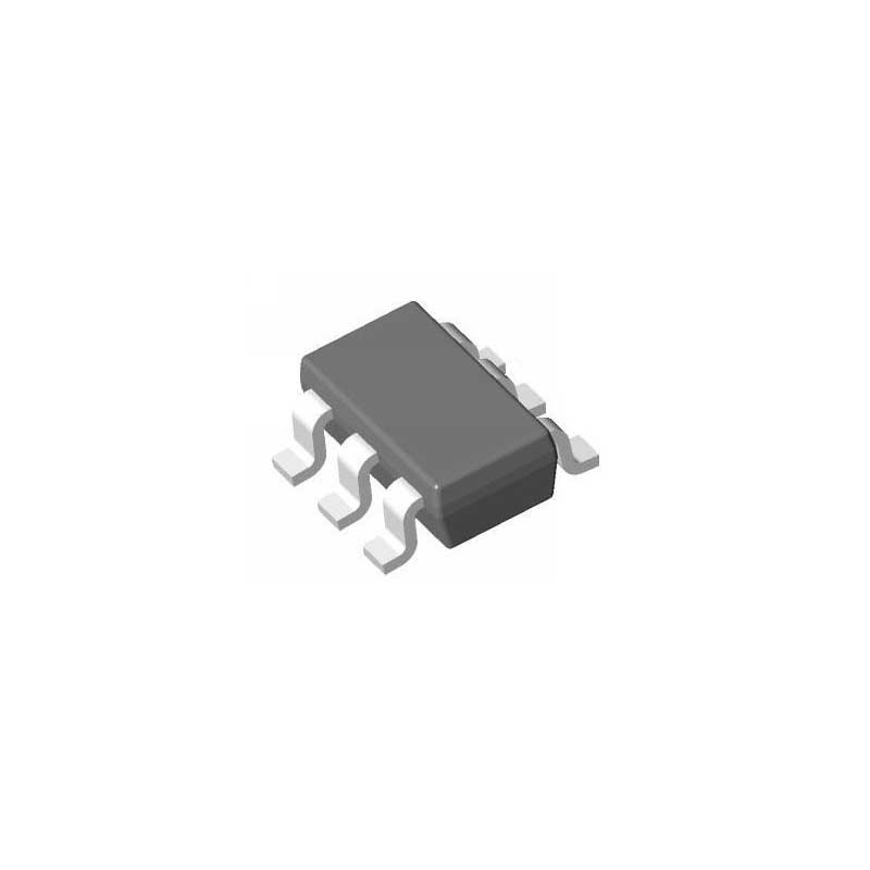
LPC824M201JHI33
For OEMs and contract manufacturers only
EPM240T100C5N
192 Macro Cells

LPC824M201JHI33K
32-bit ARM microcontroller offering affordability
