
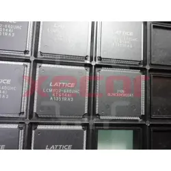
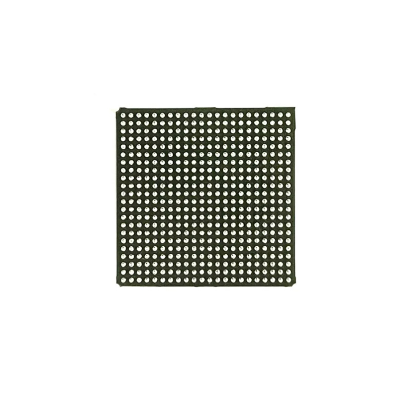
LCMXO3LF-9400C-5BG256I
LCMXO3LF-9400C-5BG256I is a highly customizable FPGA with 256 input/output connections suitable for a wide range of applications
| Quantity | Unit Price(USD) | Ext. Price |
|---|---|---|
| 1 | $21.883 | $21.88 |
| 200 | $8.468 | $1,693.60 |
| 500 | $8.171 | $4,085.50 |
| 1000 | $8.024 | $8,024.00 |
Inventory:7,697
- 90-day after-sales guarantee
- 365 Days Quality Guarantee
- Genuine Product Guarantee
- 7*24 hours service quarantee
-
Part Number : LCMXO3LF-9400C-5BG256I
-
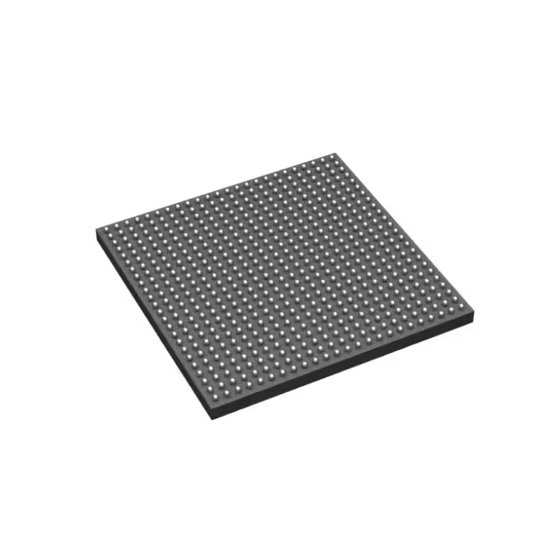
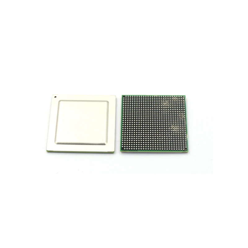
Package/Case : CSFBGA-256
-
Components Classification : FPGAs
-
Datesheet : LCMXO3LF-9400C-5BG256I DataSheet (PDF)
The LCMXO3LF-9400C-5BG256I is a low-power, low-cost, and small form-factor FPGA (Field-Programmable Gate Array) ideal for various programmable logic applications. With its integrated logic elements and flexible configuration, this FPGA offers a versatile solution for custom digital circuit designs. (Note: The pin configuration below is a general representation. Refer to the specific datasheet for precise details.) Include a circuit diagram illustrating the connections and operation of the LCMXO3LF-9400C-5BG256I FPGA for a visual representation. Note: For detailed technical specifications, please refer to the LCMXO3LF-9400C-5BG256I datasheet. Functionality The LCMXO3LF-9400C-5BG256I FPGA offers programmable logic elements that can be configured to perform a wide range of digital functions. It provides flexibility and customization for diverse application requirements. Usage Guide Q: Can the LCMXO3LF-9400C-5BG256I be reconfigured dynamically during operation? Q: What tools are recommended for programming the LCMXO3LF-9400C-5BG256I? For similar functionalities, consider these alternatives to the LCMXO3LF-9400C-5BG256I:Overview of LCMXO3LF-9400C-5BG256I
Pinout
Circuit Diagram
Key Features
Application
Frequently Asked Questions
A: Yes, this FPGA supports dynamic reconfiguration, allowing changes to logic functions while the device is operational.
A: You can use vendor-specific programming software or hardware tools provided by the FPGA manufacturer for programming and configuring the device.Equivalent
Specifications
The followings are basic parameters of the part selected concerning the characteristics of the part and categories it belongs to.
| Product Category | FPGA - Field Programmable Gate Array | RoHS | Details |
| Series | LCMXO3LF | Number of Logic Elements | 9400 LE |
| Adaptive Logic Modules - ALMs | 4700 ALM | Embedded Memory | 432 kbit |
| Number of I/Os | 206 I/O | Supply Voltage - Min | 2.375 V |
| Supply Voltage - Max | 3.465 V | Minimum Operating Temperature | - 40 C |
| Maximum Operating Temperature | + 100 C | Data Rate | 900 Mb/s |
| Mounting Style | SMD/SMT | Package / Case | CSFBGA-256 |
| Brand | Lattice | Distributed RAM | 73 kbit |
| Embedded Block RAM - EBR | 432 kbit | Maximum Operating Frequency | 400 MHz |
| Moisture Sensitive | Yes | Number of Logic Array Blocks - LABs | 1175 LAB |
| Operating Supply Voltage | 3.3 V | Product Type | FPGA - Field Programmable Gate Array |
| Factory Pack Quantity | 119 | Subcategory | Programmable Logic ICs |
| Tradename | MachXO3 | Unit Weight | 0.252788 oz |
Warranty & Returns
Warranty, Returns, and Additional Information
-
QA & Return Policy
Parts Quality Guarantee: 365 days
Returns for refund: within 90 days
Returns for Exchange: within 90 days
-
Shipping and Package
Shipping:For example, FedEx, JP, UPS, DHL,SAGAWA, or YTC.
Parts Packaging Guarantee: Featuring 100% ESD anti-static protection, our packaging incorporates high toughness and superior buffering capabilities.
-
Payment
For example, channels like VISA,MasterCard,Western Union,PayPal,MoneyGram,Rakuten Pay and more.
If you have specific payment channel preferences or requirements, please get in touch with our sales team for assistance.

LC4256ZE-7TN100I
Description: The CPLD ispMACH® 4000ZE Family offers 256 Macro Cells with a clock speed of 172MHz, operated at a 1

LC4064V-75TN44C
CPLD ispMACH4000V 64cell 168MHz TQFP44 LC4064V-75TN44C, CPLD ispMACH 4000V EEPROM 64 Cells, 30 I/O, 36 Labs, 7.5ns, ISP, 3 → 3.6 V 44-Pin TQFP

LC4128V-75TN100C
Ideal for advanced electronic applications

LCMXO2-640HC-4TG100C
LCMXO2-640HC-4TG100C Programmable Logic Device (CPLDs/FPGAs) 640 80 TQFP-100(14x14) ROHS

LCMXO2-256HC-4TG100C
Lattice Semiconductor LCMXO2-256HC-4TG100C

LC4256V-75TN144C
Programmable logic device with 256 macrocells and 400MHz speed

LCMXO2-1200HC-4SG32I
Inquire about pricing for the LCMXO2-1200HC-4SG32I unit including CoC and 2-year warranty
LCMXO640C-3FTN256C
256-pin configuration for versatile connectivity
LCMXO640C-3TN144C
Versatile field-programmable gate array with 640 logic units and 113 input/output pins
LCMXO2-640UHC-4TG144I
Green FPGA with 640 LUTs and 108 I/O in MACHX02 Series

STM32F071RBT6TR
Mainstream ARM Cortex-M0 Access line MCU with 128 Kbytes Flash and CEC functions, featuring a 48 MHz CPU
PIC12F675T-I/SN
Description of PIC12F675T-I/SN: Microcontroller with 8-bit PIC architecture, 1
AX2000-FG896I
Non-quoted descriptions for product manifestation

ADUC847BSZ62-5
MCU 8-bit 8052 CISC 62KB Flash 5V 52-Pin MQFP Tray
EP2SGX60CF780C5N
Product description: FPGA with STRATIX II GX technology
XC9572XL-10TQ100C
The XC9572XL-10TQ100C is a 100-LQFP complex programmable logic device from the XC9500XL series
STM32F415ZGT6
STM32F415ZGT6 - MCU with ARM Cortex M4F RISC architecture and 2.5V/3.3V voltage compatibility
XC6SLX45-3FGG484C
Lead-free Programmable Logic Device
STM32F301R6T6
RISC architecture for efficient processing
PIC16F819-I/SO
Embedded MCU with 3.5KB of program memory, utilizing PIC architecture and running on a 5V supply voltage