
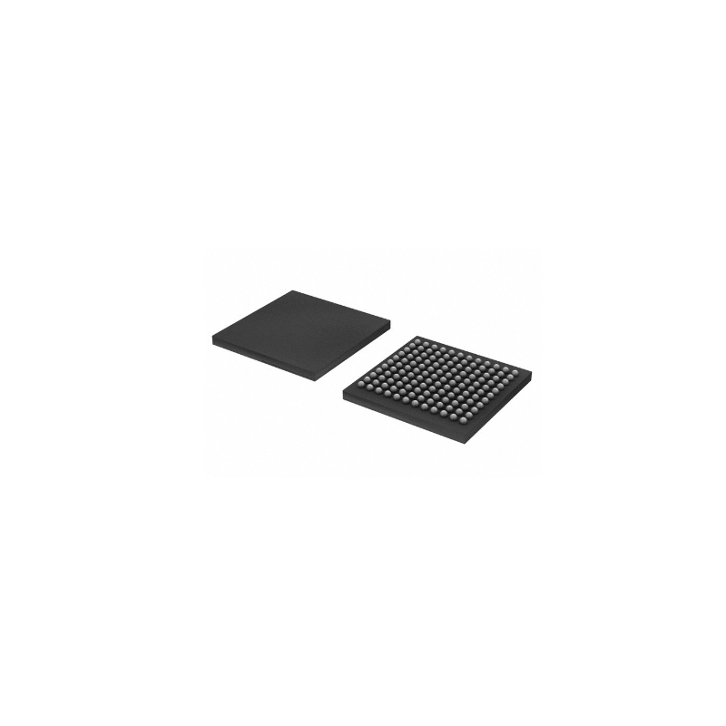
EPM570F256I5N
40 Macro Cells 201.1MHz 0.18um Technology 3.3V 256-Pin FBGA Tray
| Quantity | Unit Price(USD) | Ext. Price |
|---|---|---|
| 1 | $25.778 | $25.78 |
| 200 | $9.977 | $1,995.40 |
| 500 | $9.626 | $4,813.00 |
| 1000 | $9.452 | $9,452.00 |
Inventory:6,793
- 90-day after-sales guarantee
- 365 Days Quality Guarantee
- Genuine Product Guarantee
- 7*24 hours service quarantee
-
Part Number : EPM570F256I5N
-
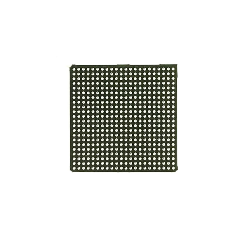
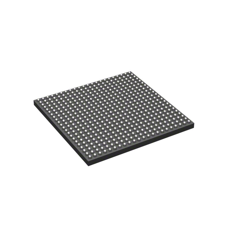
Package/Case : FBGA-256
-
Brand : Intel
-
Components Classification : CPLDs
-
Datesheet : EPM570F256I5N DataSheet (PDF)
The EPM570F256I5N is a field-programmable gate array (FPGA) integrated circuit featuring 256 macrocells and has a logic element capacity of 570 logic elements. This FPGA offers programmable functionality and versatile configuration options for various digital logic applications. (Note: The pin configuration below is a general representation. Refer to the specific datasheet for precise details.) Include a circuit diagram illustrating the connections and operation of the EPM570F256I5N FPGA for a visual representation. Note: For detailed technical specifications, please refer to the EPM570F256I5N datasheet. Functionality The EPM570F256I5N FPGA is designed to offer programmable logic functionality with a focus on flexibility and configurability. It enables efficient digital logic implementation and customization. Usage Guide Q: Can the EPM570F256I5N be reprogrammed multiple times? Q: What design software is compatible with the EPM570F256I5N? For similar FPGA options, consider these alternatives to the EPM570F256I5N:Overview of EPM570F256I5N
Pinout
Circuit Diagram
Key Features
Application
Frequently Asked Questions
A: Yes, the EPM570F256I5N FPGA is designed to support multiple reprogramming cycles for iterative design developments.
A: The EPM570F256I5N is compatible with design software such as Quartus Prime for programming and configuration purposes.Equivalent
Specifications
The followings are basic parameters of the part selected concerning the characteristics of the part and categories it belongs to.
| Product Category | CPLD - Complex Programmable Logic Devices | RoHS | Details |
| Series | EPM570 | Mounting Style | SMD/SMT |
| Package / Case | FBGA-256 | Operating Supply Voltage | 2.5 V, 3.3 V |
| Number of Macrocells | 440 Macrocell | Number of I/Os | 160 I/O |
| Supply Voltage - Max | 3.6 V | Supply Voltage - Min | 2.375 V |
| Minimum Operating Temperature | - 40 C | Maximum Operating Temperature | + 85 C |
| Maximum Operating Frequency | 304 MHz | Propagation Delay - Max | 5.4 ns |
| Brand | Intel / Altera | Memory Type | Flash |
| Moisture Sensitive | Yes | Number of Logic Array Blocks - LABs | 57 |
| Number of Logic Elements | 570 | Operating Supply Current | 55 mA |
| Product Type | CPLD - Complex Programmable Logic Devices | Factory Pack Quantity | 90 |
| Subcategory | Programmable Logic ICs | Total Memory | 8192 bit |
| Tradename | MAX II | Part # Aliases | 970394 |
Warranty & Returns
Warranty, Returns, and Additional Information
-
QA & Return Policy
Parts Quality Guarantee: 365 days
Returns for refund: within 90 days
Returns for Exchange: within 90 days
-
Shipping and Package
Shipping:For example, FedEx, JP, UPS, DHL,SAGAWA, or YTC.
Parts Packaging Guarantee: Featuring 100% ESD anti-static protection, our packaging incorporates high toughness and superior buffering capabilities.
-
Payment
For example, channels like VISA,MasterCard,Western Union,PayPal,MoneyGram,Rakuten Pay and more.
If you have specific payment channel preferences or requirements, please get in touch with our sales team for assistance.

EP2C35F484C8N
Altera FPGA EP2C35F484C8N, Cyclone II 33216 Cells, 33216 Blocks, 484-Pin FBGA

EP2S130F1020I4N
EP2S130F1020I4N product information: FPGA from the Stratix® II Family with 132540 Cells, operating at 711

EP3C16F256I7
FPGA with 963 LABs and 168 IOs

EP3C5F256C8N
Product EP3C5F256C8N description: FPGA Cyclone® III Family 5136 Cells 402MHz 65nm Technology 1.2V 256-Pin TFBGA

EPM3256ATI144-10N
Provider of electronic products in France since 1988

EPF10K130EFI484-2
Technology of 0.22um

EP4CGX30CF23C8N
Development Sample Product Description

EP4CGX150CF23I7N
Ball grid array

EP1C12Q240I7
1.5V Voltage for EP1C12Q240I7

EPF6016AQC208-3
FPGA FLEX 6000 Family 16K Gates 1320 Cells 142.86MHz 0.42um Technology 3.3V 208-Pin PQFP
XC7A35T-2CSG325C
This FPGA model, XC7A35T-2CSG325C, offers customizable logic functions and high-speed processing capabilities
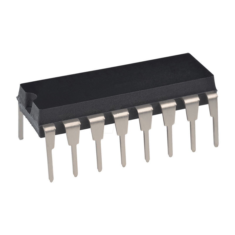
ST62T00CB6
Operating at both 3.3V and 5V, this MCU comes in a 16-Pin Plastic Dual In-line Package (PDIP) and is delivered in a convenient tube packaging
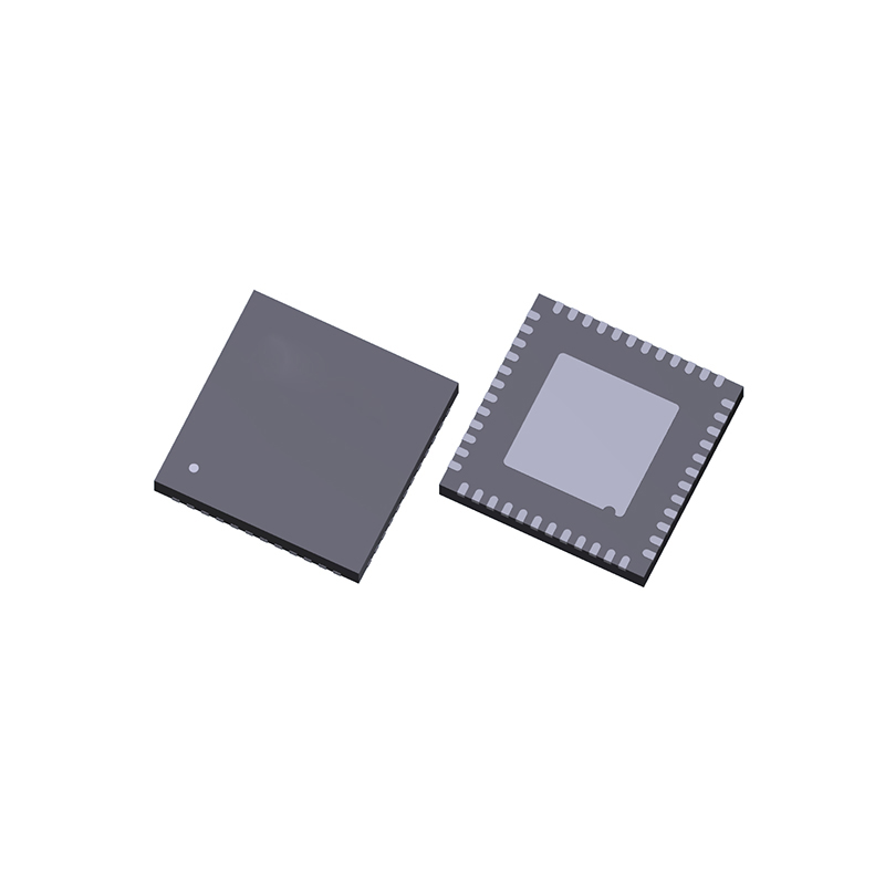
TLE9877QXA40XUMA2
MCU with 32-bit ARM Cortex M3 architecture
EPM7064STI100-7
MAX 7000 CPLD with 64 macrocells and 68 input/output ports
CY8C27243-24SXI
MCU 8-bit CY8Cxxx M8C Harvard 16KB Flash 3.3V/5V 20-Pin SOIC

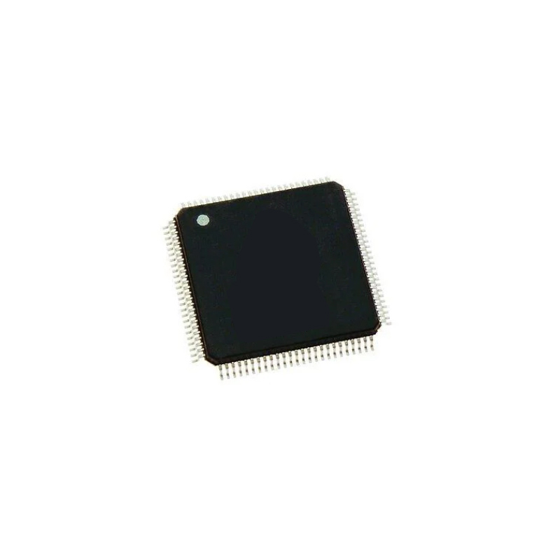
HD64F7044F28
MCU 32-bit SH-2 RISC 256KB Flash 5V 112-Pin PQFP
EP2C35F484C8N
Altera FPGA EP2C35F484C8N, Cyclone II 33216 Cells, 33216 Blocks, 484-Pin FBGA
10CX085YU484I6G
FPGA Intel 10 GX Cyclone Field Programmable Gate Array

STR911FAM44X6
High-performance STR911FAM44X6 microcontroller
10M50DCF484I7G
Family 50000 Cells