
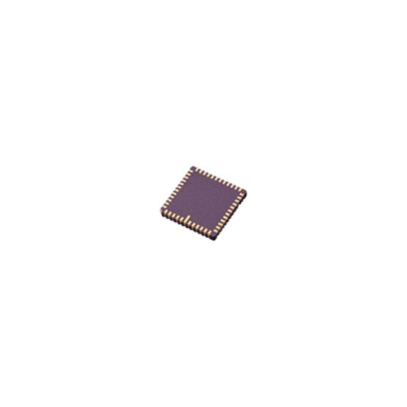
EP2C8F256C8N
256-Cell CMOS PBGA256
Inventory:9,933
- 90-day after-sales guarantee
- 365 Days Quality Guarantee
- Genuine Product Guarantee
- 7*24 hours service quarantee
-
Part Number : EP2C8F256C8N
-
Package/Case : BGA
-
Brand : Intel
-
Components Classification : FPGAs
-
Datesheet : EP2C8F256C8N DataSheet (PDF)
-
Series : CYCLONE II EP2C8
The EP2C8F256C8N is a cost-effective FPGA (Field-Programmable Gate Array) device offering a balance of performance and flexibility for various digital design applications. This FPGA features a configurable logic block architecture and embedded memory, making it suitable for prototyping, development, and production designs. (Note: The pin configuration below is a general representation. Refer to the specific datasheet for precise details.) Include a circuit diagram illustrating the connections and operation of the EP2C8F256C8N FPGA for a visual representation. Note: For detailed technical specifications, please refer to the EP2C8F256C8N datasheet. Functionality The EP2C8F256C8N FPGA provides a versatile platform for implementing custom logic functions, signal processing algorithms, and system control logic. It offers a flexible and efficient solution for digital design projects. Usage Guide Q: What programming tools are compatible with the EP2C8F256C8N? Q: Can the FPGA be reprogrammed multiple times? For similar functionalities, consider these alternatives to the EP2C8F256C8N:Overview of EP2C8F256C8N
Pinout
Circuit Diagram
Key Features
Application
Frequently Asked Questions
A: The EP2C8F256C8N is typically programmed using Quartus Prime software from Intel.
A: Yes, the EP2C8F256C8N supports reprogramming multiple times to update designs and configurations.Equivalent
Specifications
The followings are basic parameters of the part selected concerning the characteristics of the part and categories it belongs to.
| Product Category | FPGA - Field Programmable Gate Array | RoHS | Details |
| Series | Cyclone II EP2C8 | Number of Logic Elements | 8256 LE |
| Adaptive Logic Modules - ALMs | 516 ALM | Embedded Memory | 162 kbit |
| Number of I/Os | 182 I/O | Supply Voltage - Min | 1.15 V |
| Supply Voltage - Max | 1.25 V | Minimum Operating Temperature | 0 C |
| Maximum Operating Temperature | + 70 C | Mounting Style | SMD/SMT |
| Package / Case | FBGA-256 | Brand | Intel / Altera |
| Maximum Operating Frequency | 260 MHz | Moisture Sensitive | Yes |
| Number of Logic Array Blocks - LABs | 516 LAB | Operating Supply Voltage | 1.15 V to 1.25 V |
| Product Type | FPGA - Field Programmable Gate Array | Factory Pack Quantity | 90 |
| Subcategory | Programmable Logic ICs | Total Memory | 165888 bit |
| Tradename | Cyclone II | Part # Aliases | 969724 |
| Unit Weight | 1.763698 oz |
Warranty & Returns
Warranty, Returns, and Additional Information
-
QA & Return Policy
Parts Quality Guarantee: 365 days
Returns for refund: within 90 days
Returns for Exchange: within 90 days
-
Shipping and Package
Shipping:For example, FedEx, JP, UPS, DHL,SAGAWA, or YTC.
Parts Packaging Guarantee: Featuring 100% ESD anti-static protection, our packaging incorporates high toughness and superior buffering capabilities.
-
Payment
For example, channels like VISA,MasterCard,Western Union,PayPal,MoneyGram,Rakuten Pay and more.
If you have specific payment channel preferences or requirements, please get in touch with our sales team for assistance.

EP2C35F484C8N
Altera FPGA EP2C35F484C8N, Cyclone II 33216 Cells, 33216 Blocks, 484-Pin FBGA

EP2S130F1020I4N
EP2S130F1020I4N product information: FPGA from the Stratix® II Family with 132540 Cells, operating at 711

EP3C16F256I7
FPGA with 963 LABs and 168 IOs

EP3C5F256C8N
Product EP3C5F256C8N description: FPGA Cyclone® III Family 5136 Cells 402MHz 65nm Technology 1.2V 256-Pin TFBGA

EPM3256ATI144-10N
Provider of electronic products in France since 1988

EPF10K130EFI484-2
Technology of 0.22um

EP4CGX30CF23C8N
Development Sample Product Description

EP4CGX150CF23I7N
Ball grid array

EP1C12Q240I7
1.5V Voltage for EP1C12Q240I7

EPF6016AQC208-3
FPGA FLEX 6000 Family 16K Gates 1320 Cells 142.86MHz 0.42um Technology 3.3V 208-Pin PQFP
STM8S208C6T3
STM8S208C6T3 is an 8-bit microcontroller from STM8S series with CISC architecture, featuring 32KB of Flash memory and compatibility with both 3
XE167FM72F80LRABKXUMA1
MCU 16-bit C166 CISC/DSP/RISC 576KB Flash 3.3V/5V
TMS320F2802PZA
DSP Floating-Point 32bit 100MHz Automotive AEC-Q100 100-Pin LQFP Tray
PIC18F27K40-I/SO
The PIC18F27K40-I/SO is a versatile microcontroller unit optimized for a voltage range of 2.3V to 5.5V
EPM7128ELC84-15
High-density integrated circuit with 128 macrocells

TMS370C756AFNT
'TMS370C756AFNT is an 8-bit microcontroller in a 68-pin PLCC package.'
DSPIC30F6010A-20E/PF
Integrated circuit for processing with 16-bit RISC technology and 3.3V/5V compatibility
STM32F051C8T7TR
64KB Flash memory capacity
XC7Z030-1FFG676C
Integrated circuit
MKL25Z128VFT4
Versatile 32-bit MCU with 128KB Flash memory