
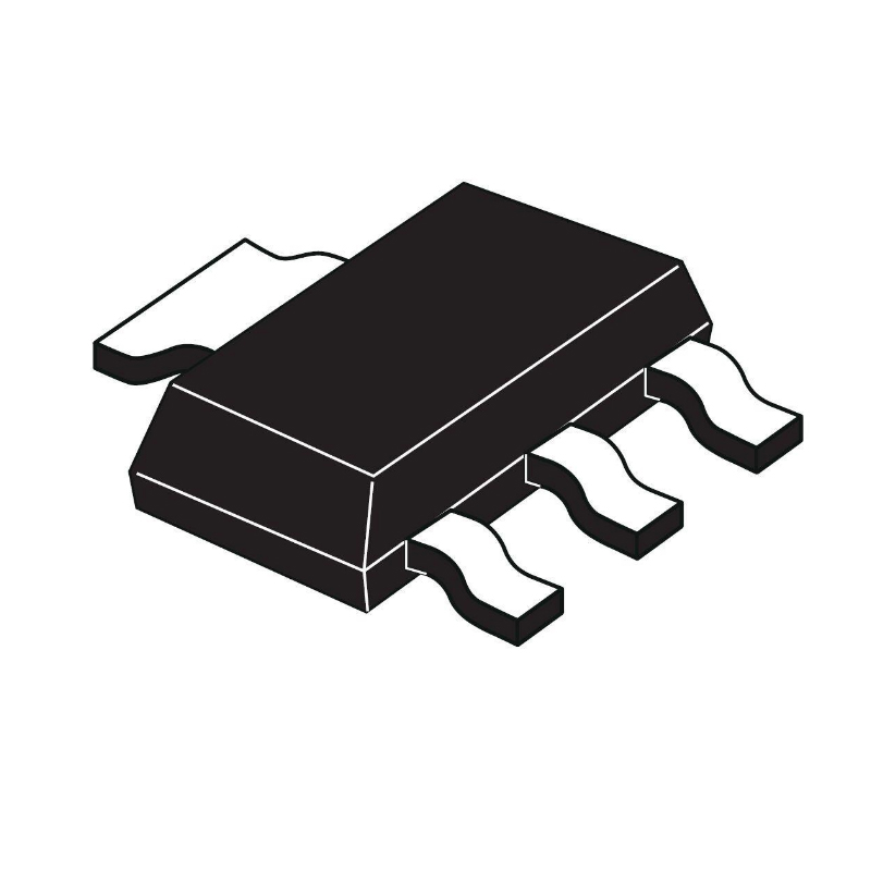
CPH3362-TL-W
SOT-23 Surface Mount Power MOSFET, Single P-Channel, 100V, 0.7A, 3.7nC
| Quantity | Unit Price(USD) | Ext. Price |
|---|---|---|
| 1 | $0.318 | $0.32 |
| 200 | $0.123 | $24.60 |
| 500 | $0.118 | $59.00 |
| 1000 | $0.117 | $117.00 |
Inventory:5,297
- 90-day after-sales guarantee
- 365 Days Quality Guarantee
- Genuine Product Guarantee
- 7*24 hours service quarantee
-
Part Number : CPH3362-TL-W
-
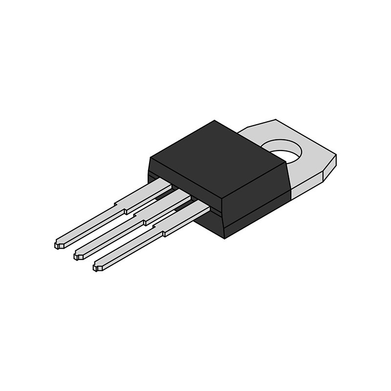
Package/Case : SOT23-3
-
Brands : Onsemi
-
Components Categories : Single FETs, MOSFETs
-
Datesheet : CPH3362-TL-W DataSheet (PDF)
The CPH3362-TL-W is a high-performance, low noise amplifier (LNA) designed for use in wireless communication systems. It is optimized for use in the 2.4GHz ISM band, providing excellent sensitivity and signal-to-noise performance for RF receivers. (Note: The pin configuration below is a general representation. Refer to the specific datasheet for precise details.) Include a circuit diagram illustrating the connections and operation of the CPH3362-TL-W LNA for a visual representation. Note: For detailed technical specifications, please refer to the CPH3362-TL-W datasheet. Functionality The CPH3362-TL-W LNA is designed to amplify and improve the reception of weak RF signals in the 2.4GHz band. It offers high gain and low noise figure, making it an essential component for sensitive wireless communication systems. Usage Guide Q: What is the typical noise figure of the CPH3362-TL-W LNA? Q: Can the CPH3362-TL-W be used in battery-powered wireless devices? For similar functionalities, consider these alternatives to the CPH3362-TL-W:Overview of CPH3362-TL-W
Pinout
Circuit Diagram
Key Features
Application
Frequently Asked Questions
A: The CPH3362-TL-W offers a typical noise figure of X dB, ensuring minimal signal degradation during amplification.
A: Yes, the CPH3362-TL-W's low power consumption and wide supply voltage range make it suitable for battery-powered wireless applications.Equivalent
Specifications
The followings are basic parameters of the part selected concerning the characteristics of the part and categories it belongs to.
| Product Category | MOSFET | RoHS | Details |
| Technology | Si | Mounting Style | SMD/SMT |
| Package / Case | SOT-23-3 | Transistor Polarity | P-Channel |
| Number of Channels | 1 Channel | Vds - Drain-Source Breakdown Voltage | 100 V |
| Id - Continuous Drain Current | 700 mA | Rds On - Drain-Source Resistance | 2.1 Ohms |
| Vgs - Gate-Source Voltage | - 20 V, + 20 V | Vgs th - Gate-Source Threshold Voltage | 1.2 V |
| Qg - Gate Charge | 3.7 nC | Minimum Operating Temperature | - 55 C |
| Maximum Operating Temperature | + 150 C | Pd - Power Dissipation | 1 W |
| Channel Mode | Enhancement | Series | CPH3362 |
| Brand | onsemi | Configuration | Single |
| Fall Time | 12 ns | Forward Transconductance - Min | 1 S |
| Product Type | MOSFET | Rise Time | 3.4 ns |
| Factory Pack Quantity | 3000 | Subcategory | MOSFETs |
| Transistor Type | 1 P-Channel | Typical Turn-Off Delay Time | 28 ns |
| Typical Turn-On Delay Time | 3.9 ns | Unit Weight | 0.000282 oz |
Warranty & Returns
Warranty, Returns, and Additional Information
-
QA & Return Policy
Parts Quality Guarantee: 365 days
Returns for refund: within 90 days
Returns for Exchange: within 90 days
-
Shipping and Package
Shipping:For example, FedEx, JP, UPS, or DHL.SG, or YTC.
Parts Packaging Guarantee: Featuring 100% ESD anti-static protection, our packaging incorporates high toughness and superior buffering capabilities.
-
Payment
For example, channels like VISA, MasterCard, UnionPay, Western Union, PayPal, and more.
If you have specific payment channel preferences or requirements, please get in touch with our sales team for assistance.

BCP56T1G
80V 1A NPN Bipolar Junction Transistor in SOT-223 package with 4-Pin configuration, 1500mW power dissipation, Tape and Reel packaging
CPH3456-TL-W
Transistor MOSFET N-channel Silicon 20V 3.5A 3-Pin CPH Tape/Reel

CPH6347-TL-W
High-Power MOSFET
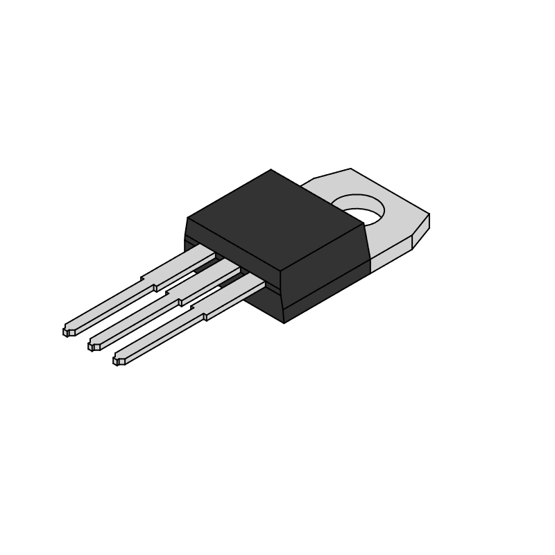
FCP22N60N
2N60N, MOSFET, N-channel, TO-220, Tube
BCP56,115
Trans GP BJT NPN 80V 1A 1350mW 4-Pin(3+Tab) SC-73 T/R
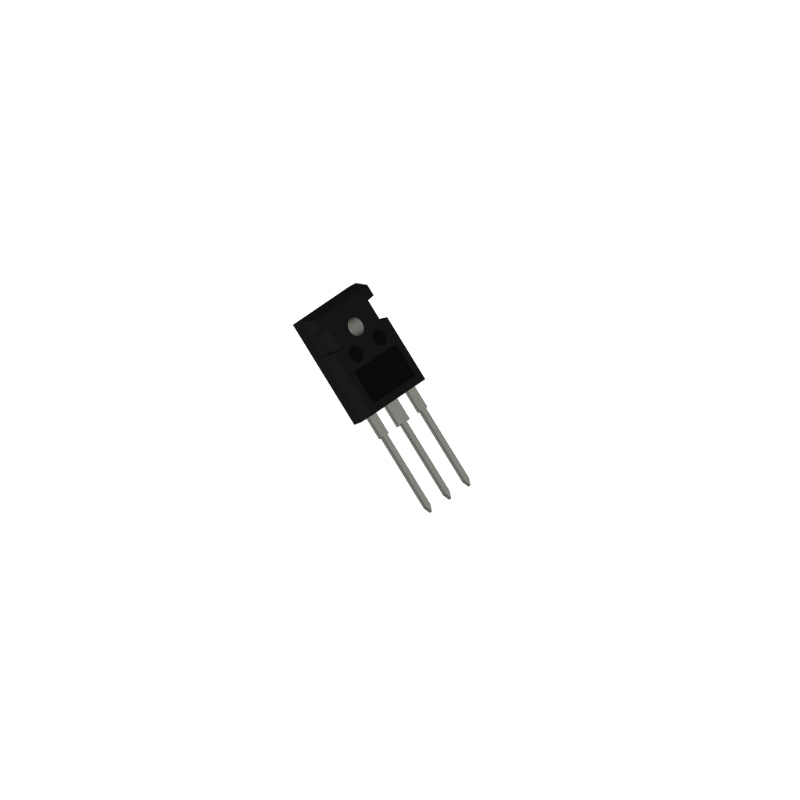
FCP11N60
Trans MOSFET N-CH 600V 11A 3-Pin(3+Tab) TO-220 Tube
IPW60R075CP
N-channel transistor MOSFET with TO-247 packaging, designed for operation at 600V and 39A
IPP60R099CP
High-voltage N-channel MOSFET transistor rated at 650V and 31A, encased in TO-220 package and supplied in tube packaging
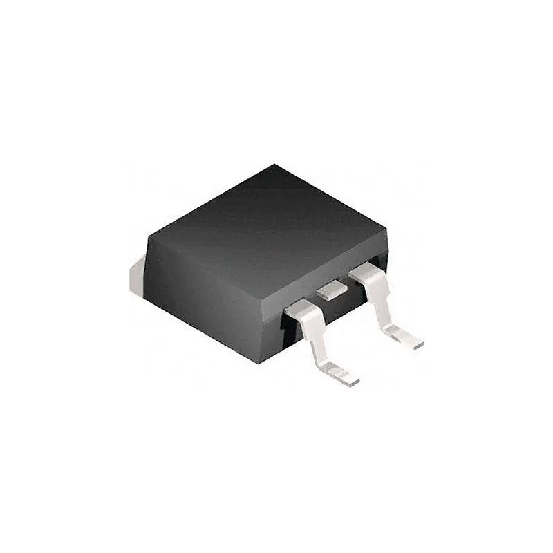
IPB60R165CP
Description: N-channel MOSFET with 650V voltage rating and 21A current capacity in D2PAK-2 package, featuring CoolMOS CP technology
IPA60R600CP
N-Channel TO-220F Transistor