
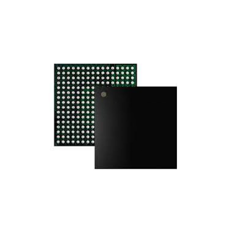
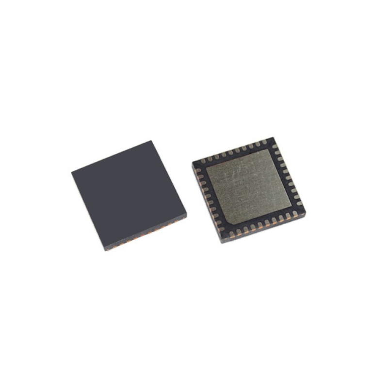
CDCM6208V1RGZT
Clock Generator 0.008MHz to 250MHz-IN 800MHz-OUT 48-Pin VQFN EP T/R
Inventory:5,178
- 90-day after-sales guarantee
- 365 Days Quality Guarantee
- Genuine Product Guarantee
- 7*24 hours service quarantee
-
Part Number : CDCM6208V1RGZT
-
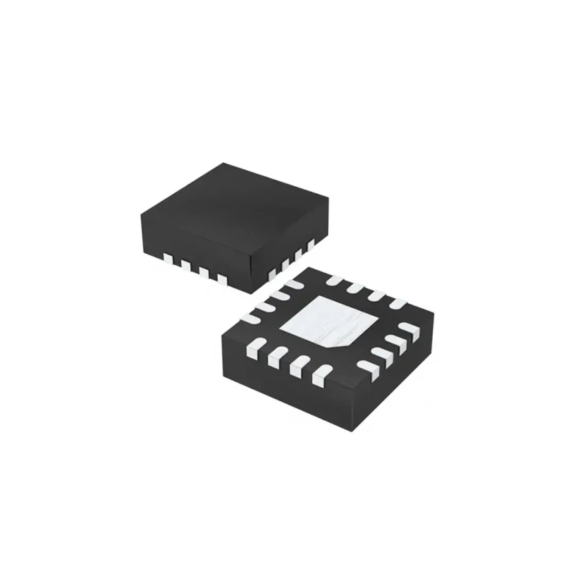
Package/Case : VQFN-48
-
Brand : Texas Instruments
-
Components Classification : Clock Generators, PLLs, Frequency Synthesizers
-
Datesheet : CDCM6208V1RGZT DataSheet (PDF)
The CDCM6208V1RGZT is a high-performance, low-jitter clock generator and distributor IC designed for use in various electronic systems. It features a wide range of output frequencies and flexible output formats, making it suitable for applications such as precision instrumentation, communication equipment, and data acquisition systems. (Note: The pin configuration below is a general representation. Refer to the specific datasheet for precise details.) Include a circuit diagram illustrating the connections and operation of the CDCM6208V1RGZT IC for a visual representation. Note: For detailed technical specifications, please refer to the CDCM6208V1RGZT datasheet. Functionality The CDCM6208V1RGZT is a high-performance clock generator and distributor that delivers low-jitter clock signals with wide frequency coverage. It offers flexible output formats and programming options to meet the requirements of diverse electronic systems. Usage Guide Q: What is the maximum output frequency supported by the CDCM6208V1RGZT? Q: Is the CDCM6208V1RGZT suitable for low-power applications? For similar functionalities, consider these alternatives to the CDCM6208V1RGZT:Overview of CDCM6208V1RGZT
Pinout
Circuit Diagram
Key Features
Application
Frequently Asked Questions
A: The CDCM6208V1RGZT supports output frequencies ranging from a few MHz to several hundred MHz, depending on the configuration and output format.
A: Yes, the CDCM6208V1RGZT operates with low power consumption, making it suitable for various low-power electronic systems requiring precision clock signals.Equivalent
Specifications
The followings are basic parameters of the part selected concerning the characteristics of the part and categories it belongs to.
| Function | Ultra-low jitter clock generator | Number of outputs | 8 |
| Output frequency (max) (MHz) | 800 | Core supply voltage (V) | 1.8, 2.5, 3.3 |
| Output supply voltage (V) | 1.8, 2.5, 3.3 | Input type | CML, LVCMOS, LVDS, LVPECL, XTAL |
| Output type | CML, HCSL, LVCMOS, LVDS, LVPECL | Operating temperature range (°C) | -40 to 85 |
| Features | I2C, Pin programmable, SPI | Rating | Catalog |
Warranty & Returns
Warranty, Returns, and Additional Information
-
QA & Return Policy
Parts Quality Guarantee: 365 days
Returns for refund: within 90 days
Returns for Exchange: within 90 days
-
Shipping and Package
Shipping:For example, FedEx, JP, UPS, DHL,SAGAWA, or YTC.
Parts Packaging Guarantee: Featuring 100% ESD anti-static protection, our packaging incorporates high toughness and superior buffering capabilities.
-
Payment
For example, channels like VISA,MasterCard,Western Union,PayPal,MoneyGram,Rakuten Pay and more.
If you have specific payment channel preferences or requirements, please get in touch with our sales team for assistance.
TS556CD
The TS556CD is a dual timer housed in a 14-pin SOIC package
TS556CDT
TS556CDT is a standard timer device with a dual temperature range of 0°C to 70°C, packaged in a 14-pin SOIC format for ease of use
CDP68HC68T1M2Z
Timekeeping peripheral for accurate time tracking

STCD1040RDM6F
Clock Distribution
4RCD0124KC0ATG
DDR4 Register Clock Driver (RCD)
CDP68HC68T1E
Real-Time Timekeeper with Memory and Power Detection

CDCE62005RGZT
The CDCE62005RGZT is a versatile clock driver with multiple output options for various applications
TS555CDT
Temperature range of 0°C to 70°C
CD4046BCN
Phase Locked Loops - PLL Phase-Locked Loop
CDCVF2505DG4
The CDCVF2505DG4 is a high-performance clock driver designed to provide precise and stable clock signals."
M41T65Q6F
M41T65Q6F, Real Time Clock, Alarm, Calendar, Clock, 16B RAM, I2C, 1.3 to 4.4V, 16-Pin QFN EP
MCP79410T-I/SN
Real Time Clock with I2C Interface and General Purpose Functions
5PB1106CMGI
LVCMOS clock buffer with temperature compensation
ADF4108BCPZ
Phase locked loops
HMC1034LP6GE
This clock generator provides a frequency range of 125MHz to 3GHz with a 3000MHz input and 40-pin QFN EP packaging for high performance
DS1021S-25+
Delay Lines / Timing Elements Programmable 8-Bit .25ns Delay Line
SI5335B-B03187-GM
Clock generation solution tailored for processors, providing a frequency of 200MHz and employing CMOS technology, packaged in a QFN-24 enclosure
SI53154-A01AGM
SILICON LABS - SI53154-A01AGM - Fanout Buffer, 100 MHz, 3.135 V to 3.465 V, 4 Outputs, QFN-24

SI5351A-B-GTR
It features a compact 10-MSOP design and has a 1.1mm dimension

DS1643-C03
DS1643-C03 offers a highly accurate timekeeping solution for embedded systems and applications