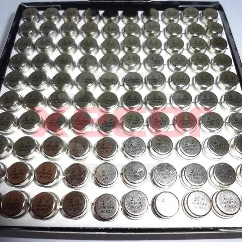
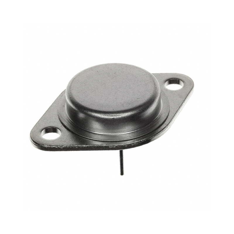
2N6849
Advanced P-channel design delivers exceptional voltage handling capabilities and spee
Inventory:9,566
- 90-day after-sales guarantee
- 365 Days Quality Guarantee
- Genuine Product Guarantee
- 7*24 hours service quarantee
-
Part Number : 2N6849
-
Package/Case : TO-205AF
-
Brand : TT ELECTRONICS
-
Components Classification : Single FETs, MOSFETs
-
Datesheet : 2N6849 DataSheet (PDF)
The 2N6849 is a P-channel JFET (junction field-effect transistor) designed for various analog and switching applications. This transistor features high input impedance, low noise, and low leakage current, making it suitable for amplification and signal processing. (Note: The pin configuration below is a general representation. Refer to the specific datasheet for precise details.) Include a circuit diagram illustrating the connections and operation of the 2N6849 transistor for a visual representation. Note: For detailed technical specifications, please refer to the 2N6849 datasheet. Functionality The 2N6849 P-channel JFET is designed to provide high input impedance and low noise characteristics for efficient signal processing and amplification tasks. Usage Guide Q: Can the 2N6849 be used in high-frequency applications? For similar functionalities, consider these alternatives to the 2N6849:Overview of 2N6849
Pinout
Circuit Diagram
Key Features
Application
Frequently Asked Questions
A: While primarily designed for low-power analog applications, the 2N6849 may have limitations in high-frequency performance. Consider alternative components for high-frequency requirements.Equivalent
Specifications
The followings are basic parameters of the part selected concerning the characteristics of the part and categories it belongs to.
| Configuration | Discrete | ID max | -6.5 A |
| Package | TO-205AF | Polarity | P |
| Qualification | DLA | VBRDSS min | -100.0 V |
| QPL Part Number | 2N6849 | RDS (on) max | 300.0 mΩ |
| Language | SPICE | Product Category | High reliability power MOSFETs |
Warranty & Returns
Warranty, Returns, and Additional Information
-
QA & Return Policy
Parts Quality Guarantee: 365 days
Returns for refund: within 90 days
Returns for Exchange: within 90 days
-
Shipping and Package
Shipping:For example, FedEx, JP, UPS, DHL,SAGAWA, or YTC.
Parts Packaging Guarantee: Featuring 100% ESD anti-static protection, our packaging incorporates high toughness and superior buffering capabilities.
-
Payment
For example, channels like VISA,MasterCard,Western Union,PayPal,MoneyGram,Rakuten Pay and more.
If you have specific payment channel preferences or requirements, please get in touch with our sales team for assistance.
2N3055-JQR-B
Bipolar power transistors with BJT technology
2N2243A
2N2243A Bipolar Transistors - BJT
2N2222AUATXV
Trans GP BJT NPN 50V 0.8A 500mW 4-Pin CSMD Waffle
2N3055-JQR-B
Bipolar power transistors with BJT technology
2N2243A
2N2243A Bipolar Transistors - BJT
2N2222AUATXV
Trans GP BJT NPN 50V 0.8A 500mW 4-Pin CSMD Waffle

2N6213
2N6213 is categorized under Bipolar Transistors, specifically Power BJT, indicating its suitability for high-power circuitry
TSM3401CX RFG
Single P-Channel MOSFET with a maximum drain current of -3A at a drain-source voltage of -30V

IXFK230N20T
MOSFETs TO-264AA ROHS

PSMN0R9-25YLC,115
MOSFET PSMN0R9-25YLC/SOT669/LFPAK
CE3514M4
MOSFETs ROHS, 125mW power capacity - Product CE3514M4
IRFD9120PBF
MOSFET P-Channel 100V 1A HVMDIP4 Vishay IRFD9120PBF P-channel MOSFET Transistor, 1 A, 100 V, 4-Pin HVMDIP
BSC670N25NSFDATMA1
The BSC670N25NSFDATMA1 MOSFET has a power dissipation of 150W at 10V and a voltage drop of 4V at a current of 90uA
ZXMN6A09G
N-channel MOSFET with enhancement mode
IPD50P04P413ATMA1
Automotive-grade P-Channel MOSFET with 40V Voltage Rating and 50A Current Capacity in DPAK Package
IRFD210PBF
200V N-channel MOSFET with HEXFET HEXDI design